
High linearity, low noise, wide bandwidth amplifier/buffer

a wide bandwidth amplifier and buffer technology, applied in the field of circuit design, can solve the problems of no circuit topology that can satisfy low noise, no high linearity, no reasonable power consumption, etc., and achieve the effect of low noise and low impedan

Active Publication Date: 2012-02-14
ATMEL CORP
View PDF7 Cites 4 Cited by
  • Summary
  • Abstract
  • Description
  • Claims
  • Application Information

AI Technical Summary

Benefits of technology

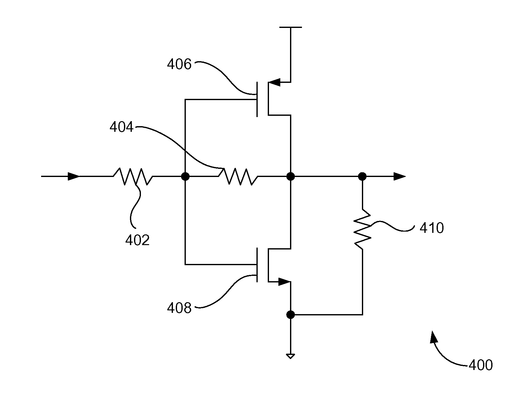
The patent text describes a radio frequency wide band amplifier architecture that has low noise and good linearity. The architecture includes a first stage amplifier and a second stage amplifier. The second stage amplifier has a lower noise level than the first stage amplifier and provides a higher linearity. The second stage amplifier includes a feedback resistor, a p-type metal-oxide-semiconductor (PMOS) transistor, and a n-type metal-oxide-semiconductor (NMOS) transistor. The architecture also includes a lumped output resistor that receives the output from the PMOS and NMOS transistors. The architecture provides a high transconductance for low input referred noise and a low impedance to limit the swing of the first stage amplifier for better linearity. The method of using the amplifier architecture includes receiving an input voltage signal, connecting a feedback resistor, and receiving an output from the feedback resistor into the PMOS and NMOS transistors. The architecture and method provide a high-quality amplifier for radio frequency applications.

Problems solved by technology

However, no circuit topologies exist that can simultaneously satisfy low noise, high linearity, reasonable power consumption and acceptable input / output matching at the same time.
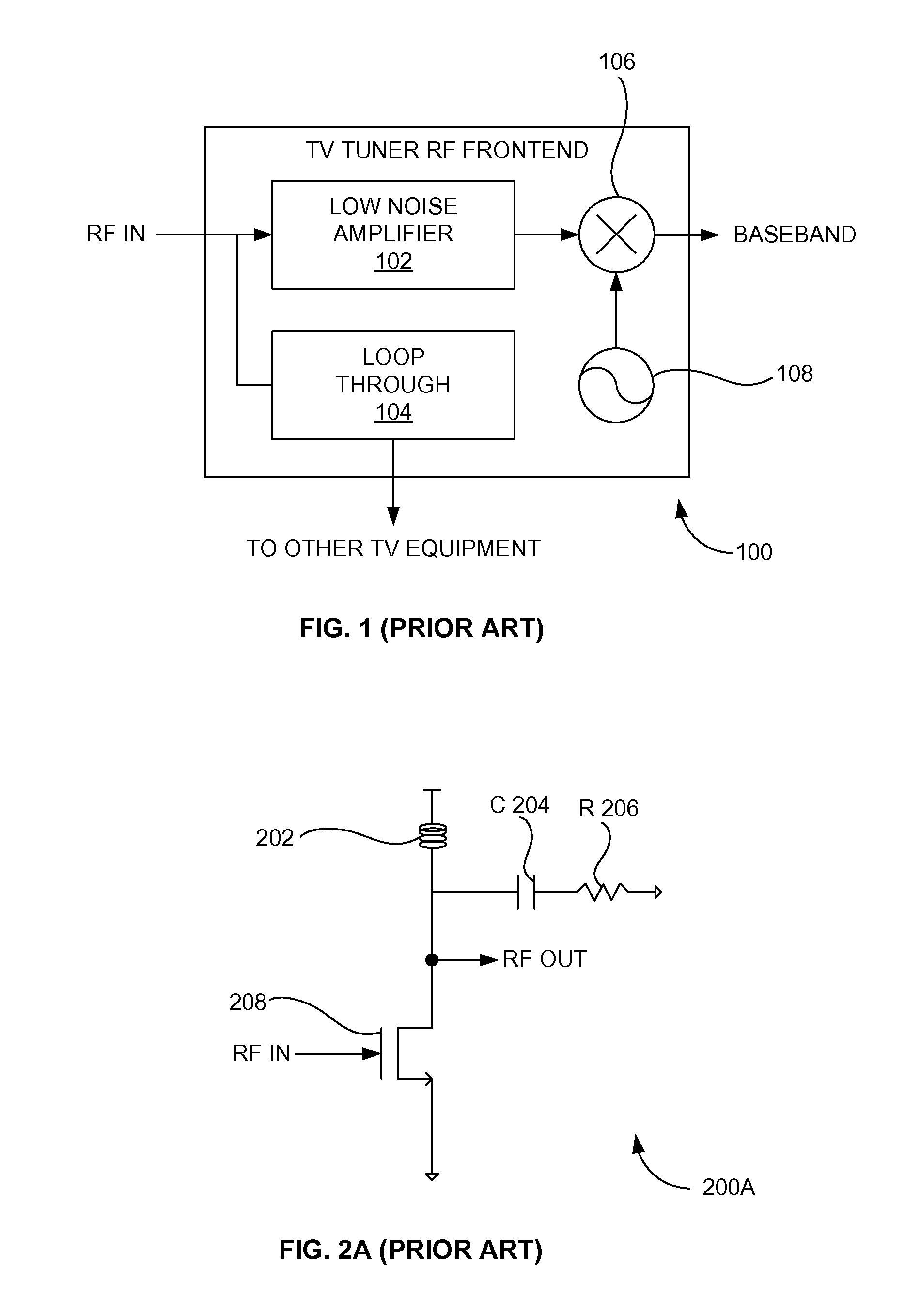
However, the loop through functions are carrying noise more than 6 dB.
This is only a simple illustration showing that due to the current circuit performance limitation, customer either has to sacrifice performance or live with higher cost.
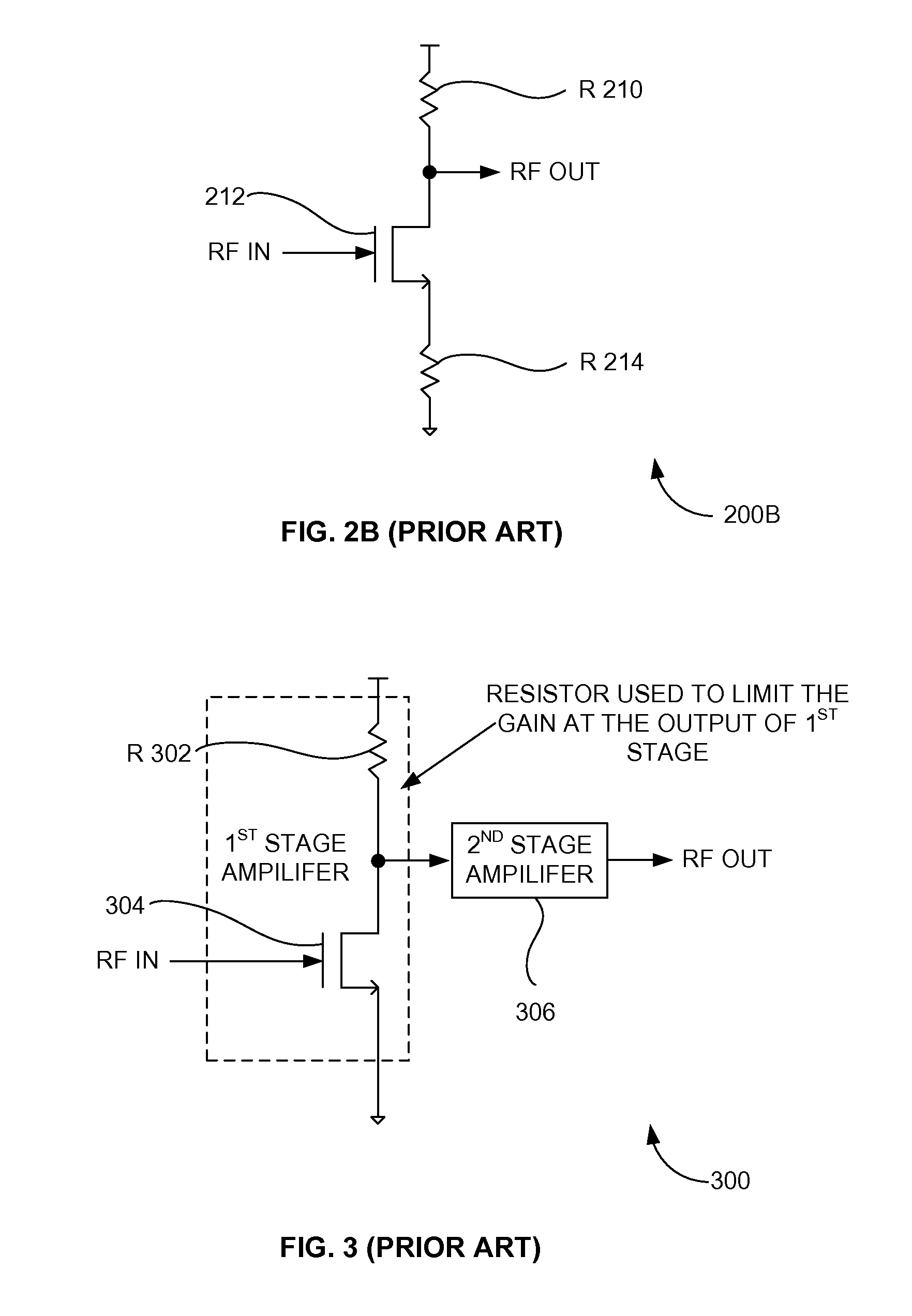
However, for a wide bandwidth amplifier at a large signal input amplitude, this gain causes distortion both at the amplifier output and the next stage where the signal level is increased.
However, because of the reduced gain, if a conventional impedance, which is a resistor, e.g., the resistor 302 is used, it will contribute noise referred to the input.
Conventional implementation may not work as the contradictory requirement of high linearity and low noise cannot be met at the same time.

Method used


Image

  • High linearity, low noise, wide bandwidth amplifier/buffer
  • High linearity, low noise, wide bandwidth amplifier/buffer
  • High linearity, low noise, wide bandwidth amplifier/buffer

Examples


Embodiment Construction

[0042]The embodiments herein and the various features and advantageous details thereof are explained more fully with reference to the non-limiting embodiments that are illustrated in the accompanying drawings and detailed in the following description. Descriptions of well-known components and processing techniques are omitted so as to not unnecessarily obscure the embodiments herein. The examples used herein are intended merely to facilitate an understanding of ways in which the embodiments herein may be practiced and to further enable those of skill in the art to practice the embodiments herein. Accordingly, the examples should not be construed as limiting the scope of the embodiments herein.

[0043]As mentioned, there remains a need to achieve low noise and high linearity at the same time and simultaneously meet the stringent requirement of low noise and high linearity. The embodiments herein achieve this by providing a noiseless impedance. More particularly, the embodiments herein ...


PUM


Abstract

A radio frequency wide band amplifier having a noise that does not exceed a threshold value, and a linearity better than a threshold value. The radio frequency wide band amplifier architecture includes a first stage amplifier and a second stage amplifier. The second stage amplifier includes an input source resistor (Rin) that receives an input voltage signal, a feedback resistor (Rfb) directly connected to the input source resistor, a p-type metal-oxide-semiconductor (PMOS) transistor directly connected to the input source resistor. The PMOS transistor receives an output from the input source resistor. A n-type metal-oxide-semiconductor (NMOS) transistor directly connected to the input source resistor. The NMOS transistor receives an output from the input source resistor. A lumped output resistor (Rout) that receives an output from the feedback resistor, the PMOS transistor, and the NMOS transistor. A terminal of the lumped output impedance is connected to ground.

Description

BACKGROUND[0001]1. Technical Field[0002]The embodiments herein generally relate to circuit design, and, more particularly, to a radio frequency wide band amplifier / buffer.[0003]2. Description of the Related Art[0004]Wide band amplifier / buffer with low noise and high linearity is desirable to save the cost of system level solution for many of today's bandwidth intensive applications. However, no circuit topologies exist that can simultaneously satisfy low noise, high linearity, reasonable power consumption and acceptable input / output matching at the same time. For example, in today's TV / cable tuner application, the loop through function process of buffering and amplifying input signal is to drive other TV / cable equipment, is preferred to be implemented on silicon to save system level solution cost. However, the loop through functions are carrying noise more than 6 dB.[0005]With a conventional approach, gain and noise can be traded off against each other. Thus, customers have the foll...

Claims


Application Information

Patent Timeline
Patent Type & Authority Patents(United States)
IPC IPC(8): H03F1/38
CPCH03F1/26H03F1/3205H03F1/342H03F3/189H03F3/193H03F3/3028H03F2200/294H03F2200/36H03F2200/411
Inventor WANG, DEJUN
Owner ATMEL CORP
Learn More