Apparatus for silencing electromagnetic noise
a technology of electromagnetic noise and apparatus, applied in the direction of line-transmission details, waveguides, semiconductor/solid-state device details, etc., can solve the problems of forming parasitic noise at the connection of the signal line and the power plane, significant increase in the complexity of the circuit layout, and reducing the cost of the integrated circuit. , the effect of eliminating the problem of signal quality and electromagnetic radiation, increasing the cost and space of the integrated circui
- Summary
- Abstract
- Description
- Claims
- Application Information
AI Technical Summary
Benefits of technology
Problems solved by technology
Method used
Image
Examples
first embodiment
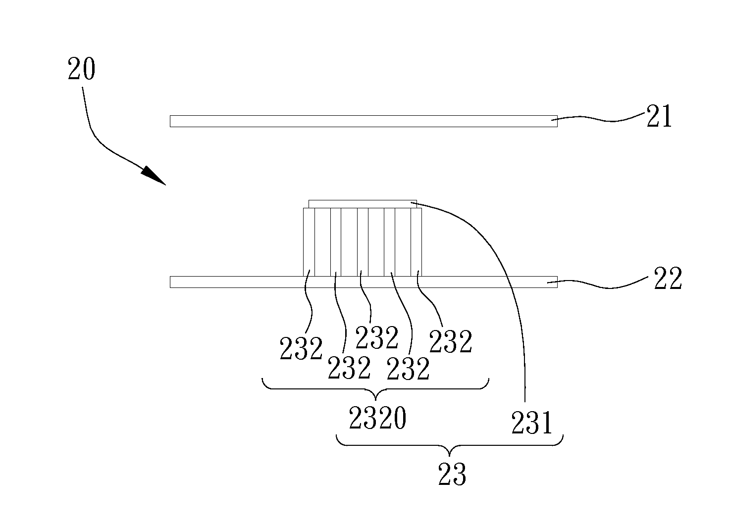
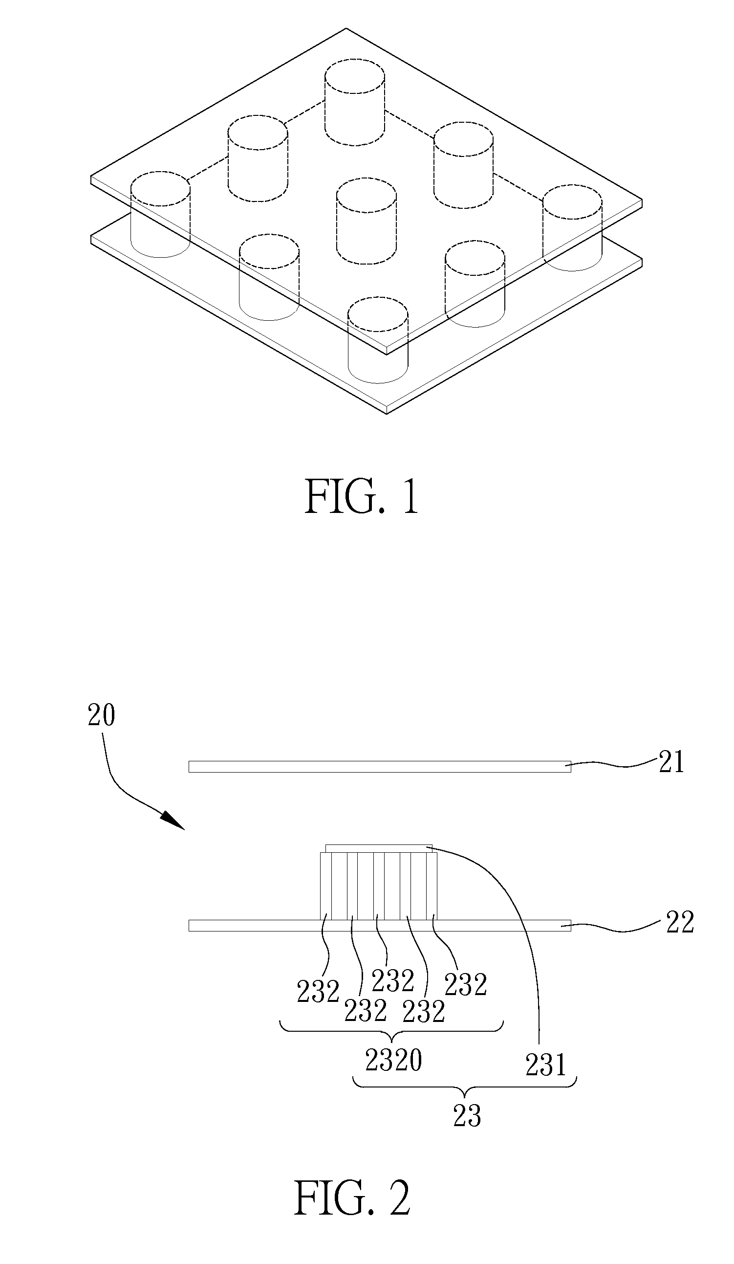
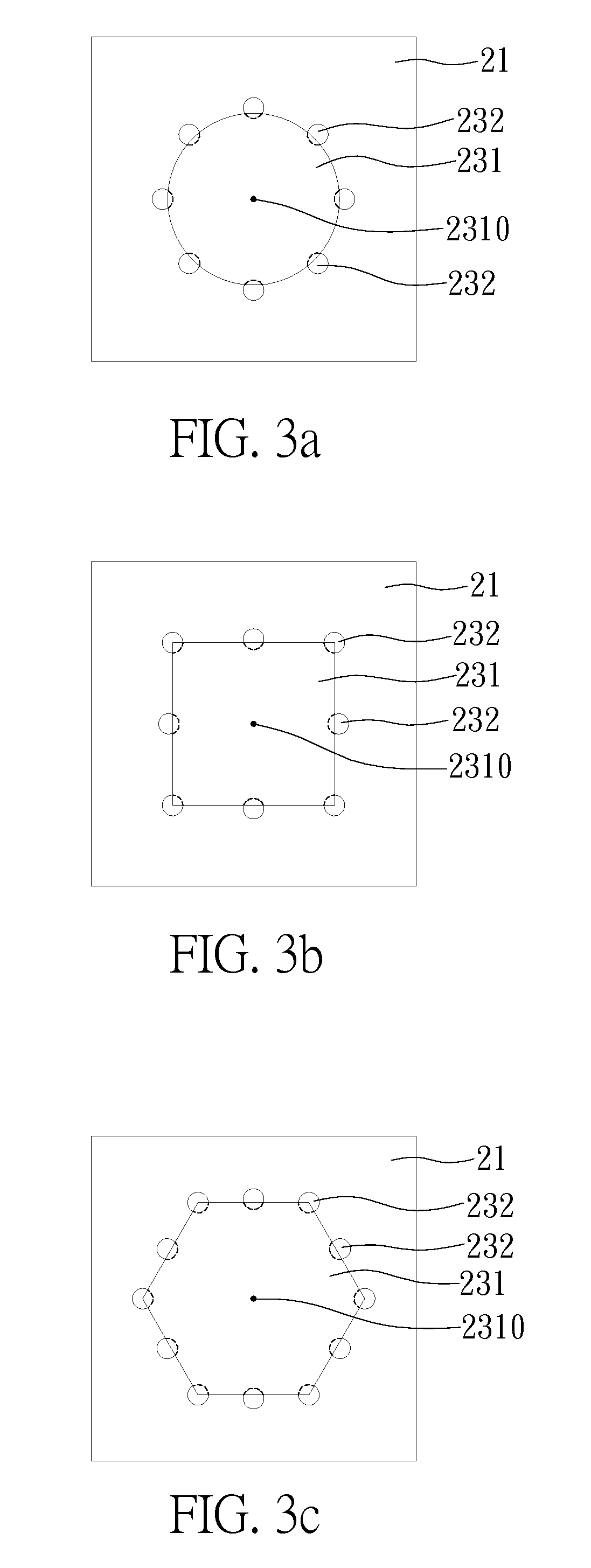
[0035]First of all, referring now to FIG. 2, a schematic view of a first embodiment of the present invention is illustrated. As shown in the diagram, an apparatus for silencing electromagnetic noise 20 of the present invention comprises at least a high voltage plane 21, a low voltage plane 22, a metal plane 231 between the high voltage plane 21 and the low voltage 22 plane, and a plurality of through via holes 232 perpendicularly coupled between the metal plane 231 and the low voltage plane 22.
[0036]In particular, the high voltage plane 21 and the low voltage plane 22 together form a pair of parallel planes, namely power plane and ground plane, respectively. The metal plane 231 is a printed circuit metallic plane coupled between the high voltage plane 21 and the low voltage plane 22.
[0037]Subsequently, considering a manufacturing process for the printed circuit, the present embodiment proposes forming blind holes by the relevant manufacturing process for the printed circuit, such th...
second embodiment
[0043]Besides, FIG. 5 is a schematic view showing a second embodiment of the present invention. As shown in the diagram, the present embodiment is derived from the same design concept of the previous embodiment. The only difference is that the apparatus for silencing electromagnetic noise 50 of the present embodiment includes a high voltage plane 51, a low voltage plane 52, two metal planes 5311, 5312 between the high voltage plane 51 and the low voltage plane 52 and a plurality of through via holes 532. Each of the through via holes 532 is perpendicularly connected between the metal plane 5311 and the metal plane 5312. The through via holes 532 are together peripherally provided on the metal plane 5311 and metal plane 5312 so as to be arranged in the form of a ring-shaped through-via-hole array structure 5320. The metal plane 5311, the metal plane 5312, and the through via holes 532 together form a ring-shaped through-via-hole crystalline unit 53.
[0044]Referring now to FIG. 6, a sc...
PUM
 Abstract
Description
Claims
Application Information
 - R&D
- Intellectual Property
- Life Sciences
- Materials
- Tech Scout
- Unparalleled Data Quality
- Higher Quality Content
- 60% Fewer Hallucinations
Browse by: Latest US Patents, China's latest patents, Technical Efficacy Thesaurus, Application Domain, Technology Topic, Popular Technical Reports.
© 2025 PatSnap. All rights reserved.Legal|Privacy policy|Modern Slavery Act Transparency Statement|Sitemap|About US| Contact US: help@patsnap.com


