Group-III nitride semiconductor device
a semiconductor and nitride technology, applied in the direction of semiconductor lasers, semiconductor laser structural details, lasers, etc., can solve the problems of reducing the emission efficiency of semiconductor light-emitting devices, difficulty in growing crystals of high quality, and failure to obtain blue light of high emission intensity, so as to achieve enhanced emission intensity, low dislocation density, and suppression of light absorption
- Summary
- Abstract
- Description
- Claims
- Application Information
AI Technical Summary
Benefits of technology
Problems solved by technology
Method used
Image
Examples
example 1
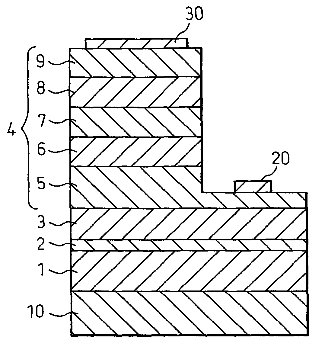
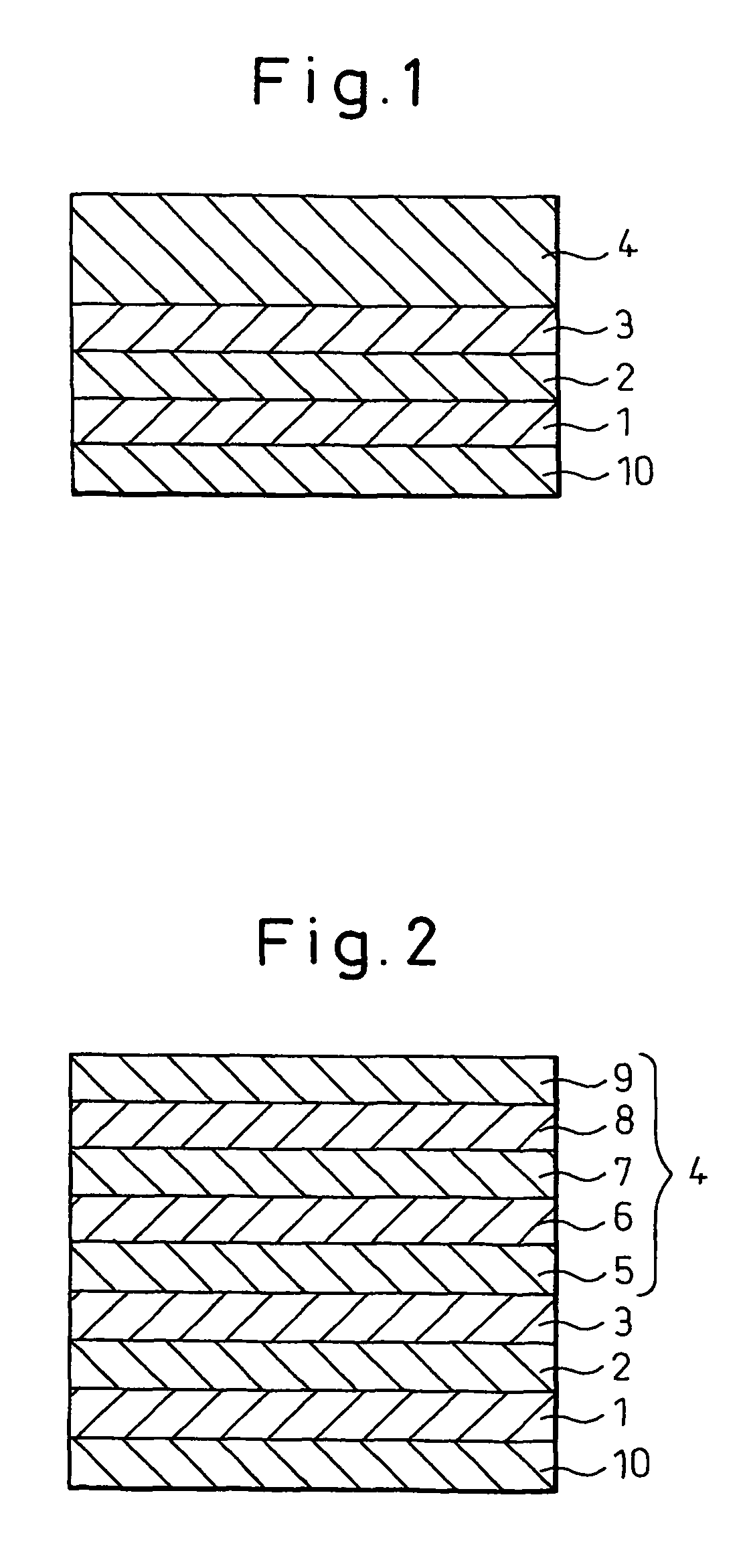
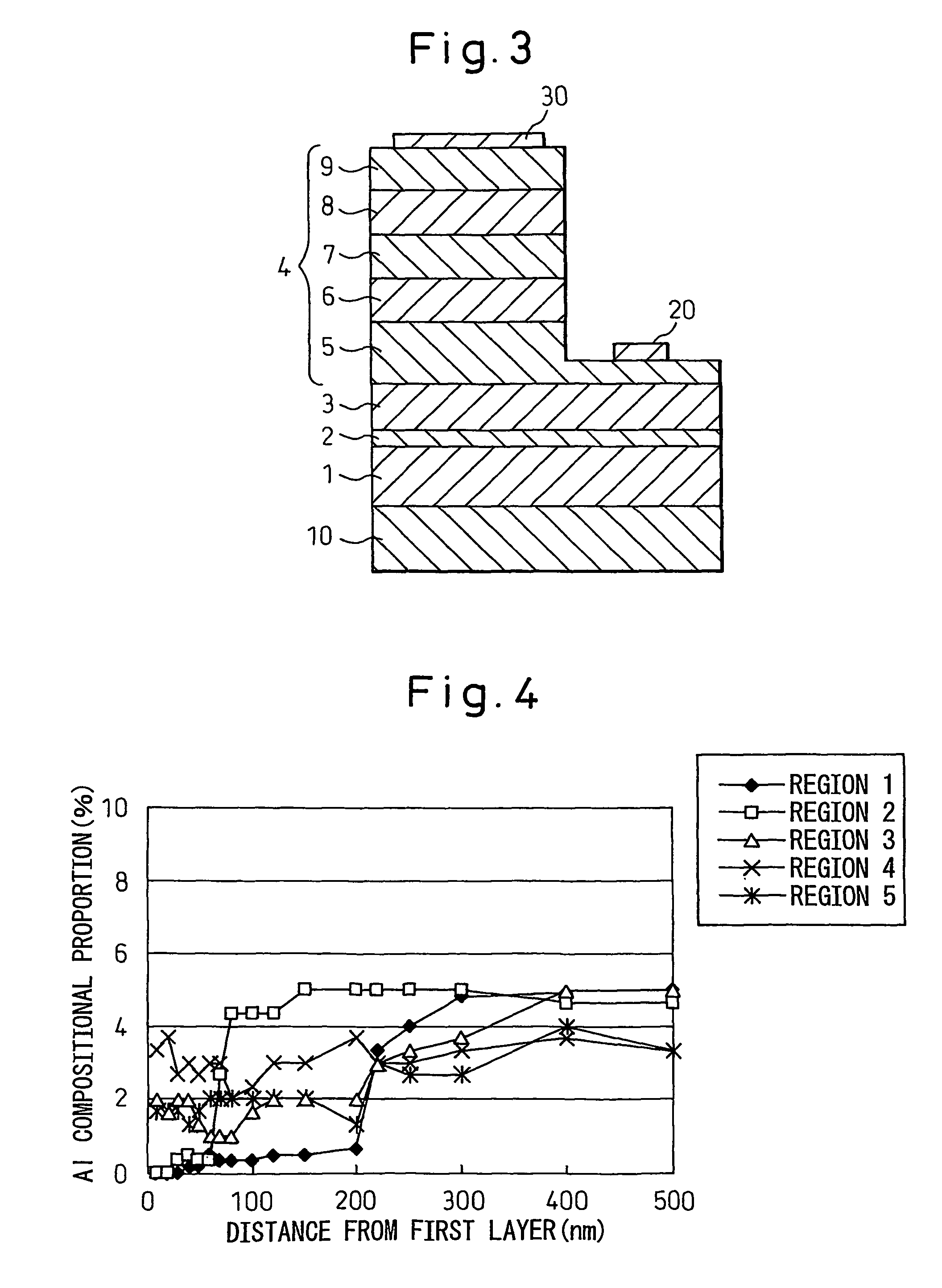
[0066]FIG. 3 is a schematic cross-sectional view showing the structure of the Group III nitride semiconductor light-emitting device produced in the present Example. The Group III nitride semiconductor light-emitting device shown in FIG. 3 was produced by successively forming semiconductor layers atop a sapphire substrate 10 through a well known MOCVD technique. The substrate 10 is a C-plane sapphire substrate having an off-angle of 0.2°. The sapphire substrate was placed in a reactor of an MOCVD growth furnace, and maintained in a hydrogen atmosphere at 1,000° C. for 10 minutes, thereby cleaning the sapphire substrate.
[0067]Subsequently, the temperature of a susceptor was increased to 1,180° C., and TMA (serving as an Al source) and NH3 (serving as an N source) were fed into the growth furnace, to thereby grow a first nitride semiconductor layer 1 formed of AlN. Specifically, H2 (serving as a carrier gas) (22 l / minute), NH3 (0.5 l / minute), and TMA (80 μmol / minute) were fed into the ...
example 2
[0076]In the present Example, a low-temperature AlN buffer layer was employed as the first nitride semiconductor layer 1. The temperature of the susceptor was regulated to 500° C., and TMA and NH3 were fed into the MOCVD growth furnace, to thereby form the AlN buffer layer. Specifically, H2 (serving as a carrier gas) (22 l / minute), NH3 (0.5 l / minute), and TMA (80 μmol / minute) were fed into the MOCVD growth furnace, and the pressure in the growth furnace was regulated to 15 kPa, to thereby form the AlN buffer layer having a thickness of about 30 nm. The procedure of Example 1 was repeated, except that the thus-formed AlN buffer layer was employed as the first nitride semiconductor layer 1, to thereby produce a light-emitting diode device. The resultant light-emitting diode device exhibited characteristics comparable to those of the light-emitting diode device of Example 1.
PUM
| Property | Measurement | Unit |
|---|---|---|
| thickness | aaaaa | aaaaa |
| thickness | aaaaa | aaaaa |
| thickness | aaaaa | aaaaa |
Abstract
Description
Claims
Application Information


