
Measurement and endpointing of sample thickness

a technology of transmission electron microscope and endpoint, which is applied in the direction of mechanical measuring arrangement, calibration apparatus, instruments, etc., can solve the problems of inability to accurately determine the endpoint of lamella creation, the complexity of the device grows, and the size of the device shrinks, so as to increase the throughput and reproducibility of tem sample creation

Active Publication Date: 2012-05-01
FEI CO
View PDF31 Cites 18 Cited by
  • Summary
  • Abstract
  • Description
  • Claims
  • Application Information

AI Technical Summary

Benefits of technology

The present invention provides improved methods for creating TEM samples, specifically by improving the endpointing process and automating it to increase throughput and reproducibility. This allows for better control and analysis of the samples, leading to better quality data. The invention can be applied to existing methods and equipment, and can be modified and adapted for different purposes.

Problems solved by technology

As features continue to get smaller and smaller, however, there comes a point where the features to be measured are too small for the resolution provided by an ordinary SEM.
Because a sample must be very thin for viewing with transmission electron microscopy (whether TEM or STEM), preparation of the sample can be delicate, time-consuming work.
Accurately determining the endpoint for lamella creation is becoming even more difficult as devices grow in complexity and shrink in size.
It is often very difficult to determine when the sample has been sufficiently thinned.
If samples are left too thick they won't be sufficiently transparent to the electrons for S / TEM analysis.
On the other hand, if the sample is thinned too much, the features to be measured or even the entire sample may be destroyed.
Even for a sample that is within the acceptable range of thickness, variation between samples is undesirable.
Even then, it is very difficult to meet any reasonable standards of reproducibility and throughput.
Even though the information that can be discovered by TEM analysis can be very valuable, the entire process of creating and measuring TEM samples has historically been so labor intensive and time consuming that it has not been practical to use this type of analysis for manufacturing process control.

Method used


Image

  • Measurement and endpointing of sample thickness
  • Measurement and endpointing of sample thickness
  • Measurement and endpointing of sample thickness

Examples


Embodiment Construction

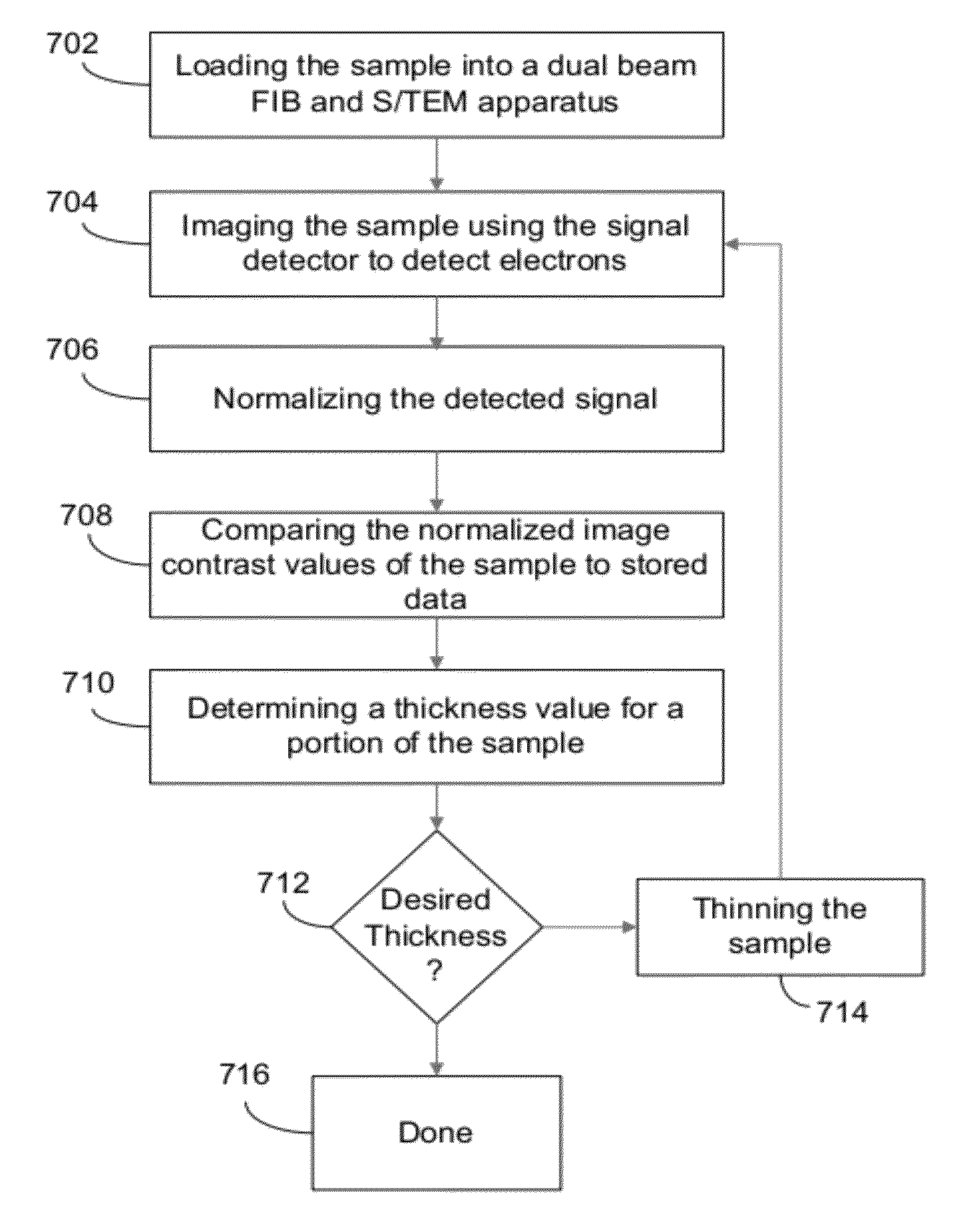
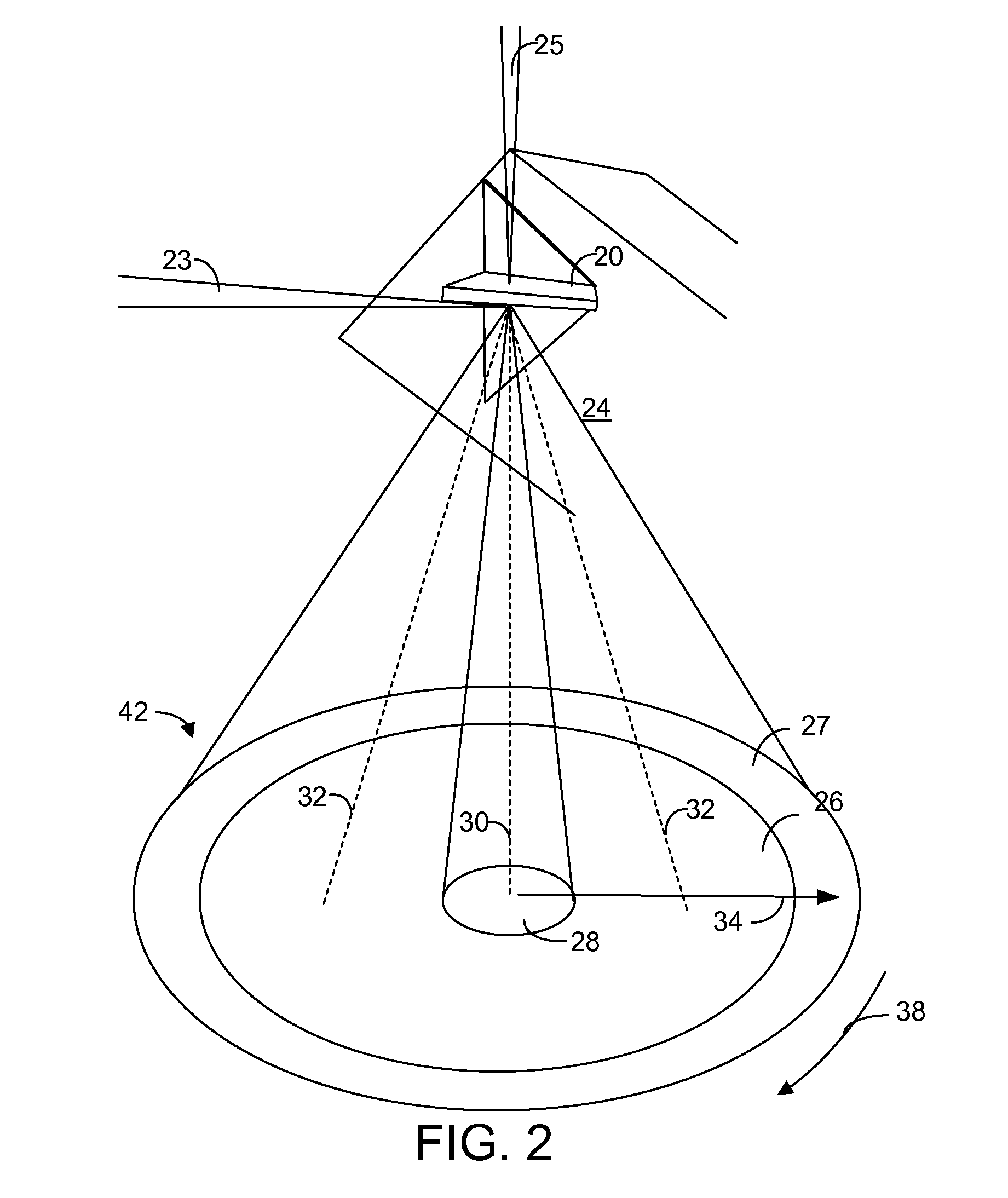
[0027]Preferred embodiments of the present invention provide improved methods for lamella creation. The use of a SEM-S / TEM detector in the dual-beam FIB / SEM allows a sample to be thinned using the FIB, while the STEM signal is used to monitor sample thickness. By mounting the sample on a pivoting sub-stage (a “flipstage”) it is possible to orient the sample for FIB thinning and then to position it for SEM-S / TEM imaging without breaking vacuum, enabling fast inspection of the thinned sample and even direct monitoring of the thinning process. Preferably, the electron beam and the ion beam can be operated at the same time (or intermittently) so thickness measurement is available during the thinning process.

[0028]A preferred embodiment of the present invention can measure the thickness of or create S / TEM samples by using a precise endpoint detection method that is reproducible and suitable for automation. Preferred embodiments also enable automatic endpointing during TEM lamella creatio...


PUM

PropertyMeasurementUnit
thickaaaaaaaaaa
angleaaaaaaaaaa
angleaaaaaaaaaa

Abstract

A method for Transmission Electron Microscopy (TEM) sample creation. The use of a Scanning Electron Microscope (SEM)—Scanning Transmission Electron Microscope (STEM) detector in the dual-beam focused ion beam (FIB) / SEM allows a sample to be thinned using the FIB, while the STEM signal is used to monitor sample thickness. A preferred embodiment of the present invention can measure the thickness of or create TEM samples by using a precise endpoint detection method. Preferred embodiments also enable automatic endpointing during TEM lamella creation and provide users with direct feedback on sample thickness during manual thinning. Preferred embodiments of the present invention thus provide methods for endpointing sample thinning and methods to partially or fully automate endpointing.

Description

[0001]This application claims priority from U.S. Provisional Pat. App. No. 61 / 110,394, filed Oct. 31, 2008, which is hereby incorporated by reference.TECHNICAL FIELD OF THE INVENTION[0002]The present invention relates to preparation of samples and methods of analysis for transmission electron microscopes and scanning transmission electron microscopes.BACKGROUND OF THE INVENTION[0003]Semiconductor manufacturing, such as the fabrication of integrated circuits, typically entails the use of photolithography. A semiconductor substrate on which circuits are being formed, usually a silicon wafer, is coated with a material, such as a photoresist, that changes solubility when exposed to radiation. A lithography tool, such as a mask or reticle, positioned between the radiation source and the semiconductor substrate casts a shadow to control which areas of the substrate are exposed to the radiation. After the exposure, the photoresist is removed from either the exposed or the unexposed areas, ...

Claims


Application Information

Patent Timeline
Patent Type & Authority Patents(United States)
IPC IPC(8): G01N23/04G06F17/00
CPCG01N1/286H01J37/304H01J37/3056H01J2237/31749H01J2237/30466H01J2237/31745H01J2237/24455
Inventor YOUNG, RICHARD J.PETERSON, BRENNANSCHAMPERS, RUDOLF JOHANNES PETER GERARDUSMORIARTY, MICHAEL
Owner FEI CO
Learn More