Front electrode for use in photovoltaic device and method of making same

a photovoltaic device and front electrode technology, applied in the direction of coatings, layered products, chemical instruments and processes, etc., can solve the problems of reducing the output power of the photovoltaic device, reducing and only having such conventional tco front electrodes, so as to reduce the reflection loss of incident solar flux, reduce visible light reflection, and increase the absorption of photons

Active Publication Date: 2012-06-19
GUARDIAN GLASS LLC
View PDF152 Cites 25 Cited by
  • Summary
  • Abstract
  • Description
  • Claims
  • Application Information

AI Technical Summary

Benefits of technology

[0002]Certain embodiments of this invention relate to a photovoltaic device including an electrode such as a front electrode / contact. In certain example embodiments of this invention, the front electrode is of or includes a transparent conductive coating (TCC) having a plurality of layers, and is provided on a surface of a front glass substrate opposite to a patterned surface of the substrate. In certain example embodiments, the patterned (e.g., etched) surface of the front transparent glass substrate faces incoming light, whereas the TCC is provided on the opposite surface of the substrate facing the semiconductor film of the photovoltaic (PV) device. In other words, the transparent glass substrate has a patterned first surface and the TCC of the front electrode is provided on the second surface thereof. The patterned first or front surface of the glass substrate reduces reflection loss of incident solar flux and increases the absorption of photon(s) in the semiconductor film through scattering, refraction and diffusion. The TCC may act to enhance transmission in selected PV active regions of the visible and near IR spectrum, while substantially rejecting and / or blocking undesired IR thermal energy from certain other areas of the spectrum.
[0003]In certain example embodiments, the front electrode of the photovoltaic device includes a multi-layer coating (or TCC) having at least one infrared (IR) reflecting and conductive substantially metallic layer of or including silver, gold, or the like, and possibly at least one transparent conductive oxide (TCO) layer (e.g., of or including a material such as tin oxide, zinc oxide, or the like). In certain example embodiments, the multilayer front electrode coating is designed to realize one or more of the following advantageous features: (a) reduced sheet resistance and thus increased conductivity and improved overall photovoltaic module output power; (b) increased reflection of infrared (IR) radiation thereby reducing the operating temperature of the photovoltaic module so as to increase module output power; (c) reduced reflection and / or increased transmission of light in the region of from about 400-700 nm, 450-700 nm, and / or 450-600 nm, which leads to increased photovoltaic module output power; (d) reduced total thickness of the front electrode coating which can reduce fabrication costs and / or time; and / or (e) improved or enlarged process window in forming the TCO layer(s) because of the reduced impact of the TCO's conductivity on the overall electric properties of the module given the presence of the highly conductive substantially metallic IR reflecting layer(s).

Problems solved by technology

Unfortunately, photovoltaic devices (e.g., solar cells) with only such conventional TCO front electrodes suffer from the following problems.
A lower sheet resistance may be achieved by increasing the thickness of such a TCO, but this will cause transmission of light through the TCO to drop thereby reducing output power of the photovoltaic device.
This IR radiation causes heat which increases the operating temperature of the photovoltaic device thereby decreasing the output power thereof.
Third, conventional TCO front electrodes such as pyrolytic tin oxide tend to reflect a significant amount of light in the region of from about 400-700 nm, or 450-700 nm, so that less than about 80% of useful solar energy reaches the semiconductor absorbing layer; this significant reflection of visible light is a waste of energy and leads to reduced photovoltaic module output power.
Fourth, the rather high total thickness (e.g., 400 nm) of the front electrode in the case of a 400 nm thick tin oxide TCO, leads to high fabrication costs.
In this respect, even small changes in the process window can adversely affect conductivity of the TCO.
When the TCO is the sole conductive layer of the front electrode, such adverse affects can be highly detrimental.

Method used


Image

  • Front electrode for use in photovoltaic device and method of making same
  • Front electrode for use in photovoltaic device and method of making same
  • Front electrode for use in photovoltaic device and method of making same

Examples


Embodiment Construction

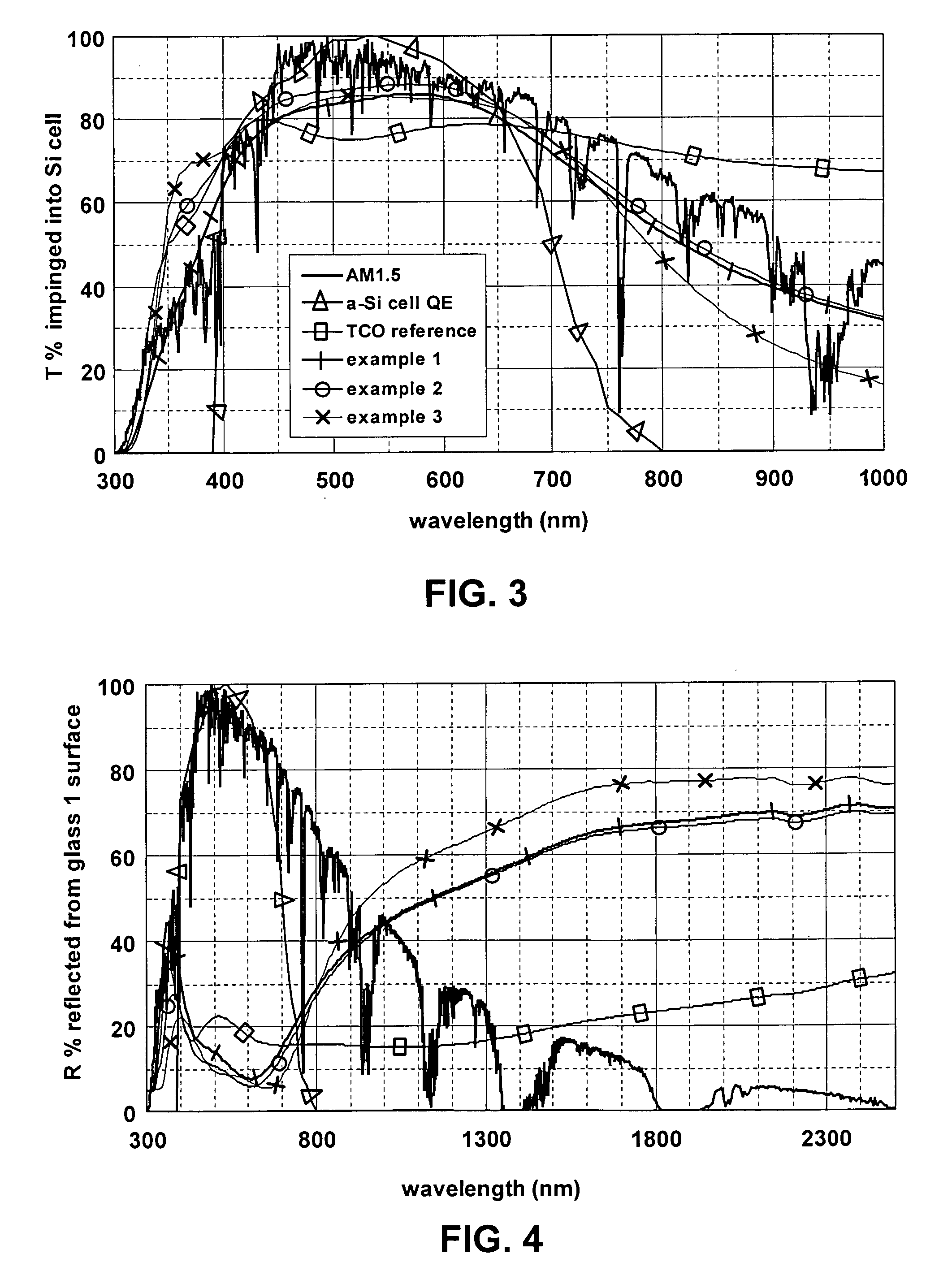
of this invention (having a textured front surface of the front glass substrate) versus comparative examples; this shows that the Example 4 of this invention realized increased transmission in the approximately 500-700 nm wavelength range and thus increased photovoltaic module output power, compared to the comparative example without the etched front surface (x dotted line) and the comparative example of the conventional TCO superstrate (o solid line).

DETAILED DESCRIPTION OF EXAMPLE EMBODIMENTS OF THE INVENTION

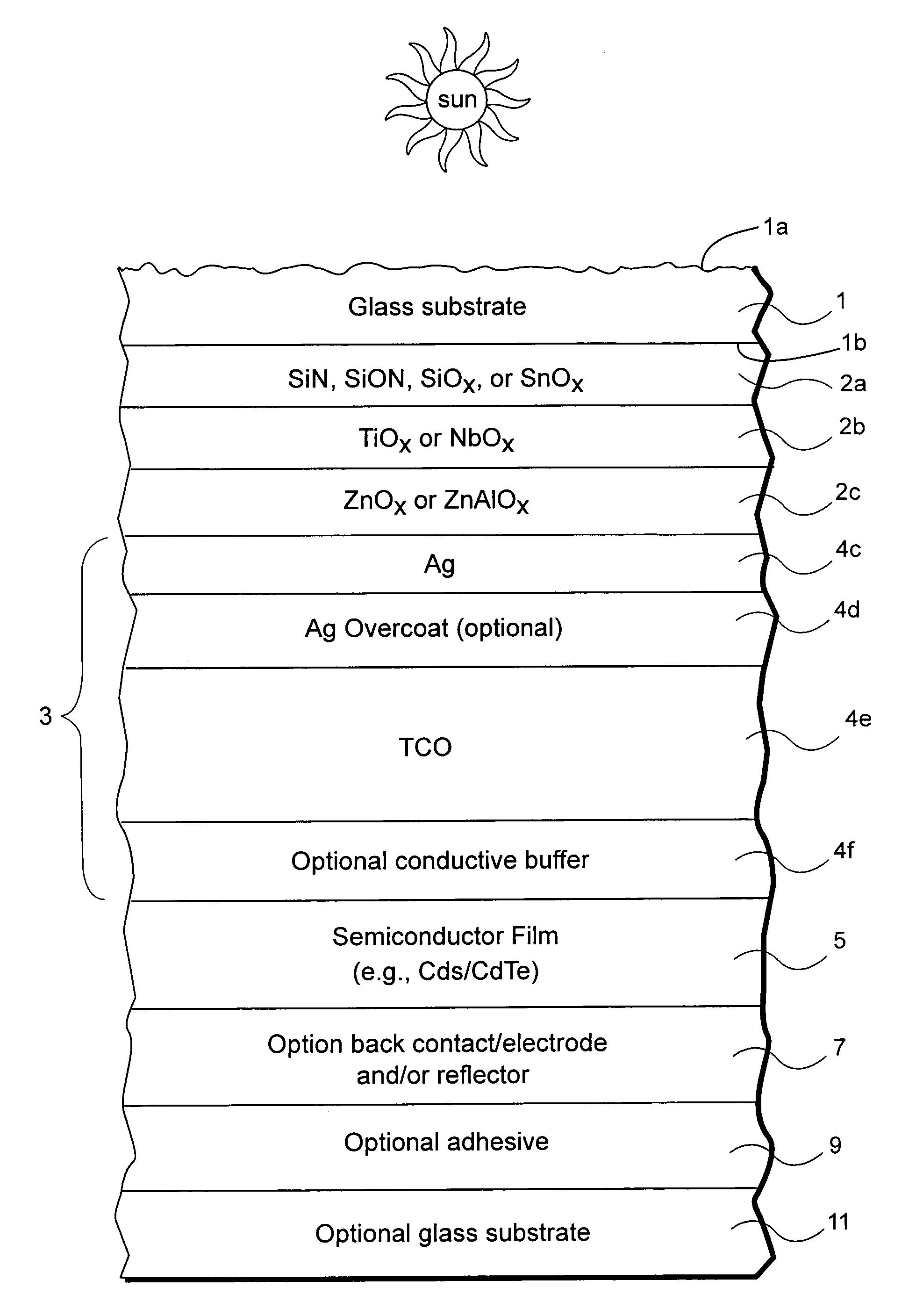
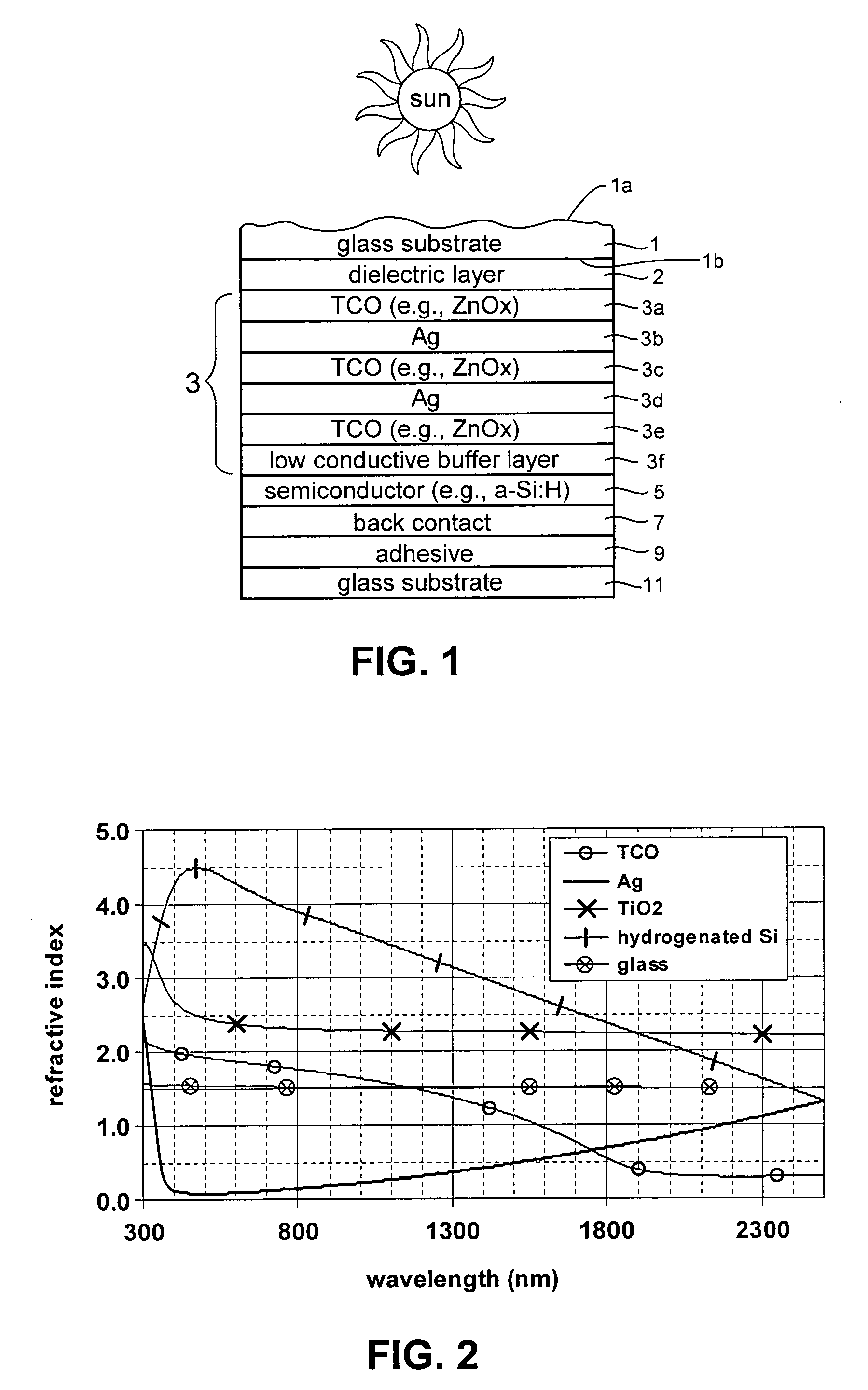
[0032]Referring now more particularly to the figures in which like reference numerals refer to like parts / layers in the several views.

[0033]Photovoltaic devices such as solar cells convert solar radiation into usable electrical energy. The energy conversion occurs typically as the result of the photovoltaic effect. Solar radiation (e.g., sunlight) impinging on a photovoltaic device and absorbed by an active region of semiconductor material (e.g., a semiconductor film including...


PUM

PropertyMeasurementUnit
surface roughnessaaaaaaaaaa
refractive indexaaaaaaaaaa

Abstract

This invention relates to a front electrode / contact for use in an electronic device such as a photovoltaic device. In certain example embodiments, the front electrode of a photovoltaic device or the like includes a multilayer coating including at least one transparent conductive oxide (TCO) layer (e.g., of or including a material such as tin oxide, ITO, zinc oxide, or the like) and / or at least one conductive substantially metallic IR reflecting layer (e.g., based on silver, gold, or the like). In certain example instances, the multilayer front electrode coating may include one or more conductive metal(s) oxide layer(s) and one or more conductive substantially metallic IR reflecting layer(s) in order to provide for reduced visible light reflection, increased conductivity, cheaper manufacturability, and / or increased infrared (IR) reflection capability. At least one of the surfaces of the front glass substrate may be textured in certain example embodiments of this invention.

Description

[0001]This application is a continuation-in-part (CIP) of each of U.S. Ser. Nos. 11 / 984,092, filed Nov. 13, 2007, 11 / 987,664, filed Dec. 3, 2007, 11 / 898,641, filed Sep. 13, 2007, 11 / 591,668, filed Nov. 2, 2006, and 11 / 790,812, filed Apr. 27, 2007, the entire disclosures of which are all hereby incorporated herein by reference.[0002]Certain embodiments of this invention relate to a photovoltaic device including an electrode such as a front electrode / contact. In certain example embodiments of this invention, the front electrode is of or includes a transparent conductive coating (TCC) having a plurality of layers, and is provided on a surface of a front glass substrate opposite to a patterned surface of the substrate. In certain example embodiments, the patterned (e.g., etched) surface of the front transparent glass substrate faces incoming light, whereas the TCC is provided on the opposite surface of the substrate facing the semiconductor film of the photovoltaic (PV) device. In other...

Claims


Application Information

Patent Timeline
Patent Type & Authority Patents(United States)
IPC IPC(8): H01L31/00
CPCH01L31/02168H01L31/022425H01L31/022466B32B17/10036B32B17/10229Y02E10/50H01L31/022483
Inventor LU, YIWEIDEN BOER, WILLEMLERIN, DAVIDTHOMSEN, SCOTT V.
Owner GUARDIAN GLASS LLC
Why Eureka
Try Eureka