Ferroelectric material, method of producing ferroelectric material, and ferroelectric device
a technology of ferroelectric material and thin film, which is applied in the direction of thin/thick film capacitors, devices, solid-state devices, etc., can solve the problems of difficult use of bfo in room-temperature environment, the effect of affecting the performance of bfo, and the effect of good ferroelectricity
- Summary
- Abstract
- Description
- Claims
- Application Information
AI Technical Summary
Benefits of technology
Problems solved by technology
Method used
Image
Examples
example 1
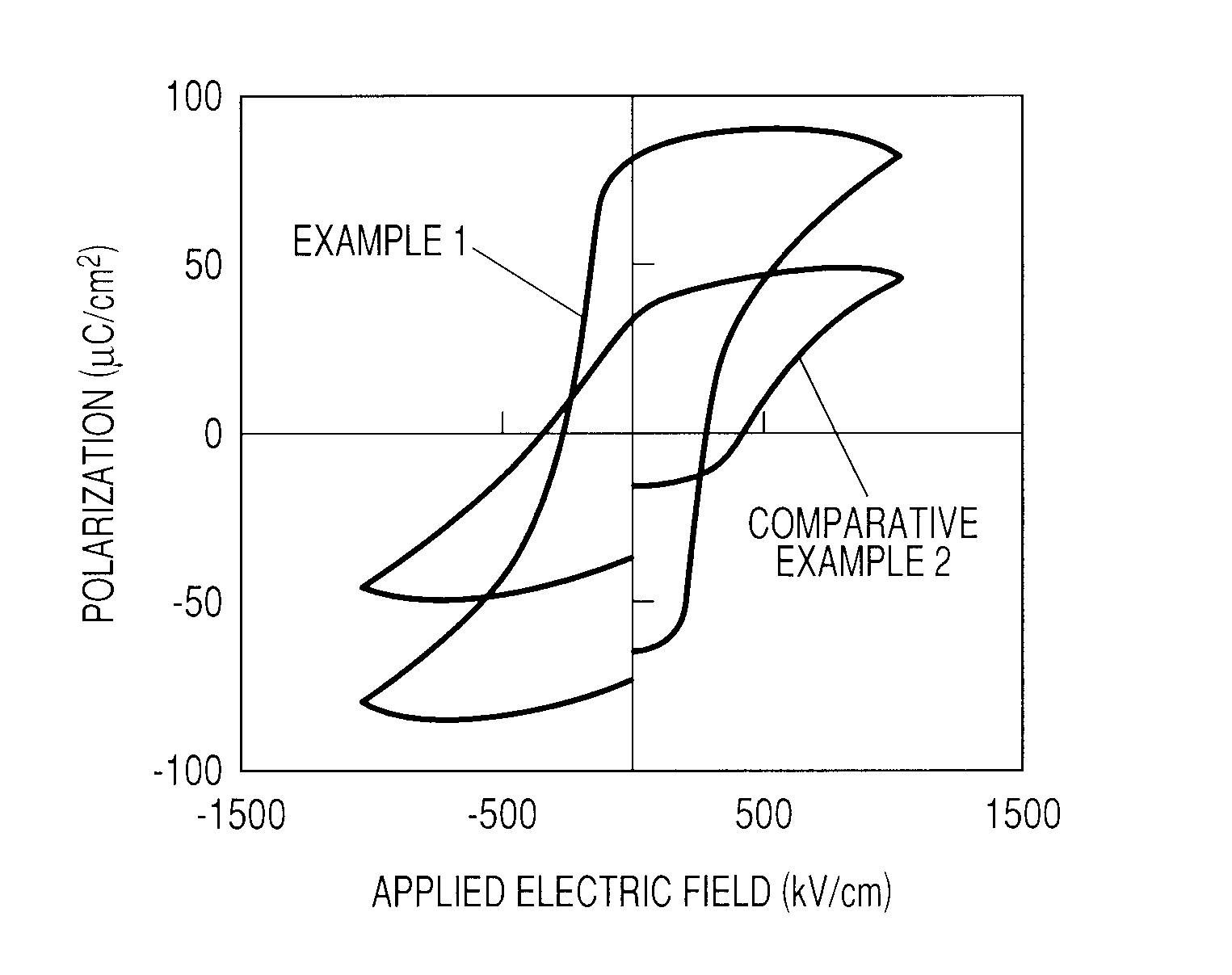
[0076]A metal oxide thin film was formed on a substrate by a chemical solution deposition method involving the use of the raw material mixed solution of Production Example 1.
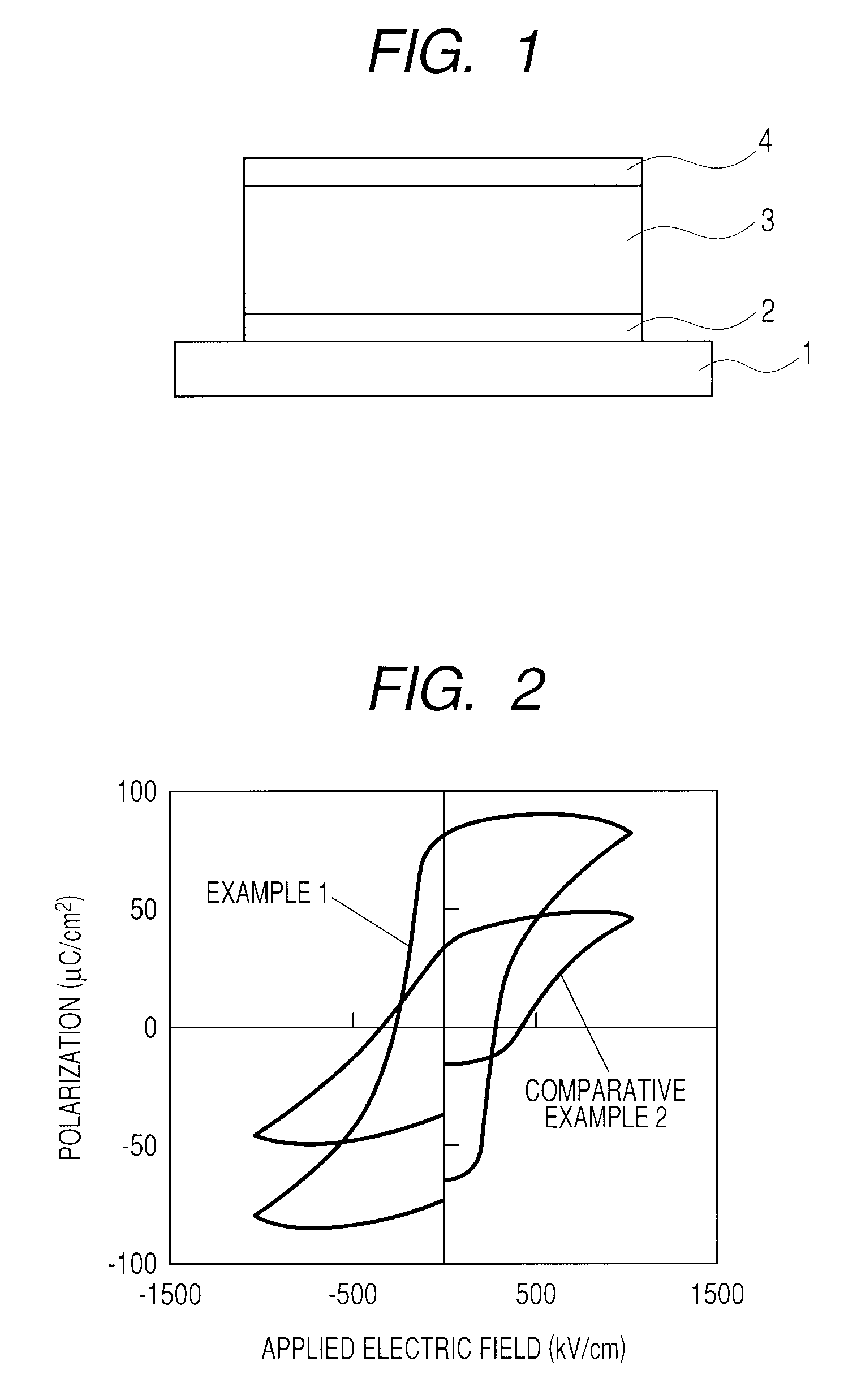
[0077]As the substrate on which the thin film is formed, a silicon substrate with an oxide film having a platinum titanium alloy with a thickness of about 100 nm on a film formation plane as a lower electrode was used.
[0078]First, the raw material mixed solution 1 was applied onto the above substrate with a spin coater (6,000 rpm). The applied layer was thermally treated under an air atmosphere. The heat treatment process was performed with a hot plate in two stages, i.e., 150° C. for 1 minute and 350° C. for 3 minutes.
[0079]After that, the application process and the heat treatment process were similarly repeated so that second to sixth layers might be formed. Finally, the entire substrate was thermally treated at 650° C. for 5 minutes so that a film might be crystallized. As a result, the ferroelectric thin fi...
examples 2 to 9
[0084]Ferroelectric thin films were each formed on the substrate by using each of the raw material mixed solutions of Production Examples 2 to 9 in the same manner as in Example 1 except the number of coating layers.
[0085]XRD found that each of those ferroelectric thin films had a rhombohedral perovskite-type crystal structure.
[0086]In addition, each of the thin films was evaluated for the number of coating layers, a thickness measured with a contact displacement meter, an average particle diameter measured with an AFM, the abundance ratio of a metal element determined by XRF, and the presence or absence of tetravalent manganese. The results are as shown in Table 2.
PUM
| Property | Measurement | Unit |
|---|---|---|
| particle diameter | aaaaa | aaaaa |
| thickness | aaaaa | aaaaa |
| thickness | aaaaa | aaaaa |
Abstract
Description
Claims
Application Information

