All-solid-state reflective dimming electrochromic device having buffer layer and dimmer member using the same
a technology of electrochromic devices and solid-state reflective, which is applied in the direction of liquid surface applicators, instruments, coatings, etc., can solve the problems of increasing costs, radiated into the interior, and reducing comfort in the vehicle, so as to achieve high transmittance and enable switching in a short time over a wide area
- Summary
- Abstract
- Description
- Claims
- Application Information
AI Technical Summary
Benefits of technology
Problems solved by technology
Method used
Image
Examples
example 1
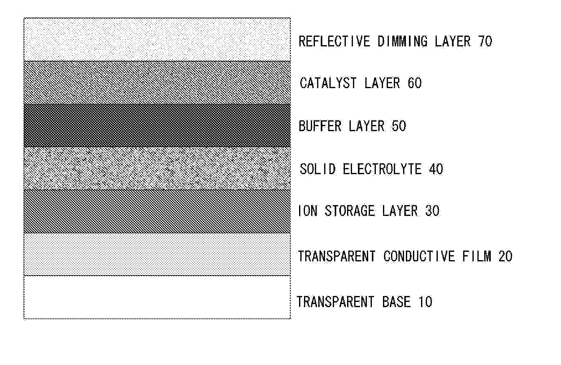
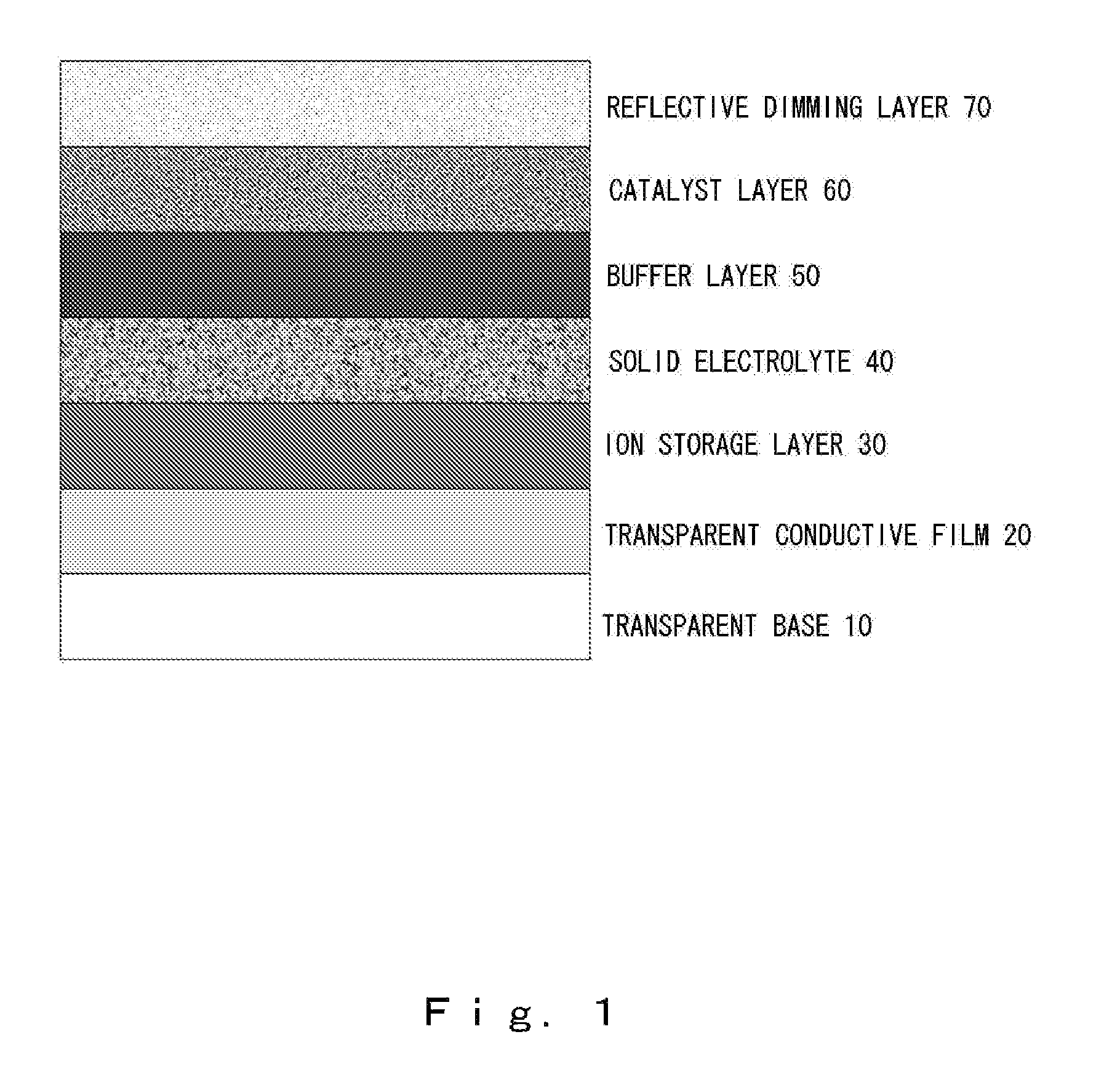
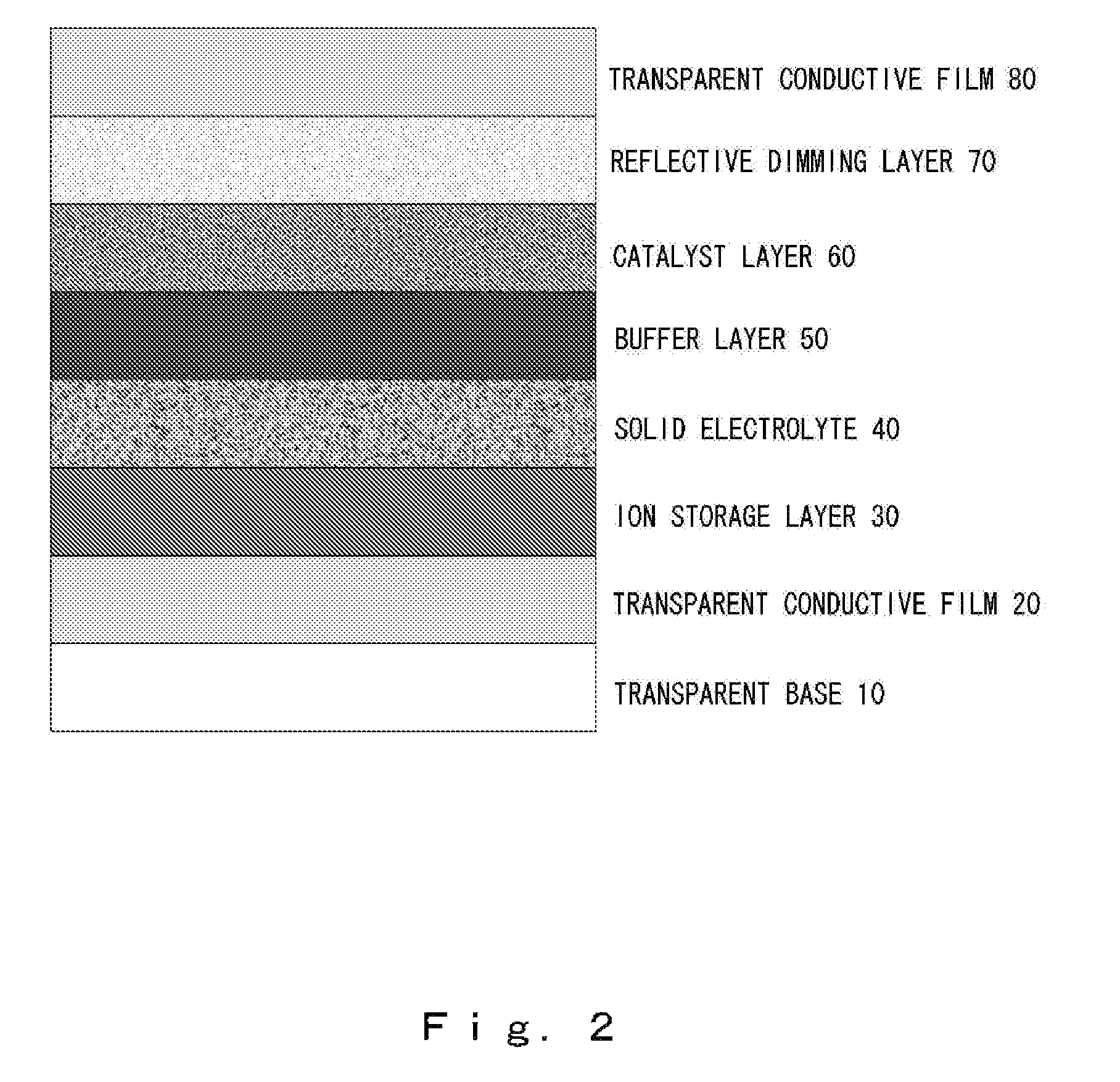
[0107]First, an explanation is provided of a first example of the present invention with reference to FIG. 1. An all-solid-state reflective dimming electrochromic device shown in FIG. 1 was produced in this example. Although the following provides an explanation of the order of steps of one embodiment of a manufacturing method, the technical scope of the present invention is not limited to the following process. For example, an electrochromic device can be produced by forming a transparent conductive film, a reflective dimming layer and a catalyst layer on a first base, and forming a transparent conductive film, an ion storage layer and a solid electrolyte layer on a second base, followed by lamination thereof.
[0108]A glass sheet coated with a transparent conductive film in the form of tin-doped indium oxide and having surface resistance of 10 Ω / □ and thickness of 1 mm was used as a base. After washing the base, it was placed in a vacuum device and air was evacuated to draw a vacuum...
example 2
[0118]A two-layer film consisting of tantalum oxide and tungsten oxide was produced by following the same procedure as that of Example 1 followed by vapor-depositing a buffer layer in the form of an aluminum thin film on the surface thereof by DC sputtering. Argon was used for the atmospheric gas, and sputtering was carried out by setting the pressure in the pressure chamber to 0.6 Pa and applying power of 50 W to an aluminum metal target. The film thickness of the resulting aluminum buffer layer was about 2 nm.
[0119]Vapor deposition of a palladium catalyst layer and a magnesium-titanium alloy thin film reflective dimming layer on the surface of the three-layer film consisting of aluminum vapor-deposited for the buffer layer, tantalum oxide and tungsten oxide with a three-way magnetron sputtering system. Targets consisting of titanium metal, nickel metal and palladium metal were respectively placed on the three sputter guns. During deposition, the palladium was sputtered first follo...
example 3
[0125]A two-layer film consisting of tantalum oxide and tungsten oxide was produced by following the same procedure as that of Example 1 followed by vapor-depositing a buffer layer in the form of an aluminum thin film on the surface thereof by DC sputtering. Argon was used for the atmospheric gas, and sputtering was carried out by setting the pressure in the pressure chamber to 0.6 Pa and applying power of 50 W to an aluminum metal target. The film thickness of the resulting aluminum buffer layer was about 2 nm.
[0126]Vapor deposition of a palladium catalyst layer and a magnesium-niobium alloy thin film reflective dimming layer on the surface of the three-layer film consisting of aluminum vapor-deposited for the buffer layer, tantalum oxide and tungsten oxide with a three-way magnetron sputtering system. Targets consisting of niobium metal, nickel metal and palladium metal were respectively placed on the three sputter guns. During deposition, the palladium was sputtered first followe...
PUM
| Property | Measurement | Unit |
|---|---|---|
| density | aaaaa | aaaaa |
| light transmittance | aaaaa | aaaaa |
| temperatures | aaaaa | aaaaa |
Abstract
Description
Claims
Application Information


