Sputtering target, transparent conductive film, and transparent electrode for touch panel

a technology of conductive film and electrode, applied in the direction of diaphragm, metallic material coating process, conductive materials, etc., can solve the problems of difficult reduction of indium content, achieve high bulk resistance, increase bulk resistance, and reduce relative density

Active Publication Date: 2012-11-06
IDEMITSU KOSAN CO LTD
View PDF15 Cites 31 Cited by
  • Summary
  • Abstract
  • Description
  • Claims
  • Application Information

AI Technical Summary

Benefits of technology

[0027]This oxide may contain, in addition to the hexagonal layered compound and the spinel structure compound, a bixbyite structure, a wurtzite structure compound and a rutile structure compound. Further, insofar as the advantageous effects of the invention are not impaired, in addition to indium, tin and zinc, the sputtering target of the invention may also contain aluminum, gallium, magnesium, boron, germanium, niobium, molybdenum, tungsten, yttrium, antimony, hafnium, tantalum, calcium, beryllium, strontium, cesium and lanthanoids.
[0028]The target of the invention preferably has an atomic ratio of In / (In+Sn+Zn) in a range of 0.10 to 0.35, preferably in a range of 0.11 to 0.29, more preferably 0.12 to 0.24, and particularly preferably 0.14 to 0.24.
[0029]If the atomic ratio of In / (In+Sn+Zn) is less than 0.10, the target may have a low relative density and a high bulk resistance. If more than 0.35, indium reduction may be insufficient.
[0030]The target of the invention preferably has an atomic ratio of Sn / (In+Sn+Zn) in a range of 0.15 to 0.35, preferably 0.18 to 0.34, and more preferably 0.20 to 0.33. If the atomic ratio is outside of the above-mentioned range, there is a possibility that the hexagonal layered structure compound of In2O3(ZnO)m, wherein m is an integer of 3 to 9, and the spinel structure compound of Zn2SnO4 cannot be included in the target at the same time, and the target may have an increased bulk resistance.
[0031]The target of the invention preferably has an atomic ratio of Zn / (In+Sn+Zn) in a range of 0.50 to 0.70, preferably 0.51 to 0.69, and more preferably 0.52 to 0.65. If the atomic ratio is outside of the above-mentioned range, there is a possibility that the hexagonal layered structure compound of In2O3(ZnO)m, wherein m is an integer of 3 to 9, and the spinel structure compound of Zn2SnO4 cannot be included in the target at the same time, and the target may have an increased bulk resistance.
[0032]In the sputtering target of the invention, in an X-ray diffraction (XRD), it is preferred that the maximum peak intensity of the hexagonal layered compound of In2O3(ZnO)m (I(In2O3(ZnO)m)), the maximum peak intensity of the spinel structure compound of Zn2SnO4 (I(Zn2SnO4)), and the maximum peak intensity of the rutile structure compound of SnO2 (I(SnO2)) satisfy the following relationship:(I(In2O3(ZnO)m)) / (I(Zn2SnO4))<1(I(SnO2)) / (I(In2O3(ZnO)m))<1(I(SnO2)) / (I(Zn2SnO4))<1It is preferred that (I(In2O3(ZnO)m)) / (I(Zn2SnO4)) be smaller than 0.3. Outside the above-mentioned range, the target may have an increased bulk resistance.

Problems solved by technology

That is, in a target formed of IZO, increasing relative density and lowering bulk resistance cannot be attained simultaneously, and therefore, reduction of the indium content is difficult.

Method used


Image

  • Sputtering target, transparent conductive film, and transparent electrode for touch panel
  • Sputtering target, transparent conductive film, and transparent electrode for touch panel

Examples


example 1

(1) Production of Sputtering Target

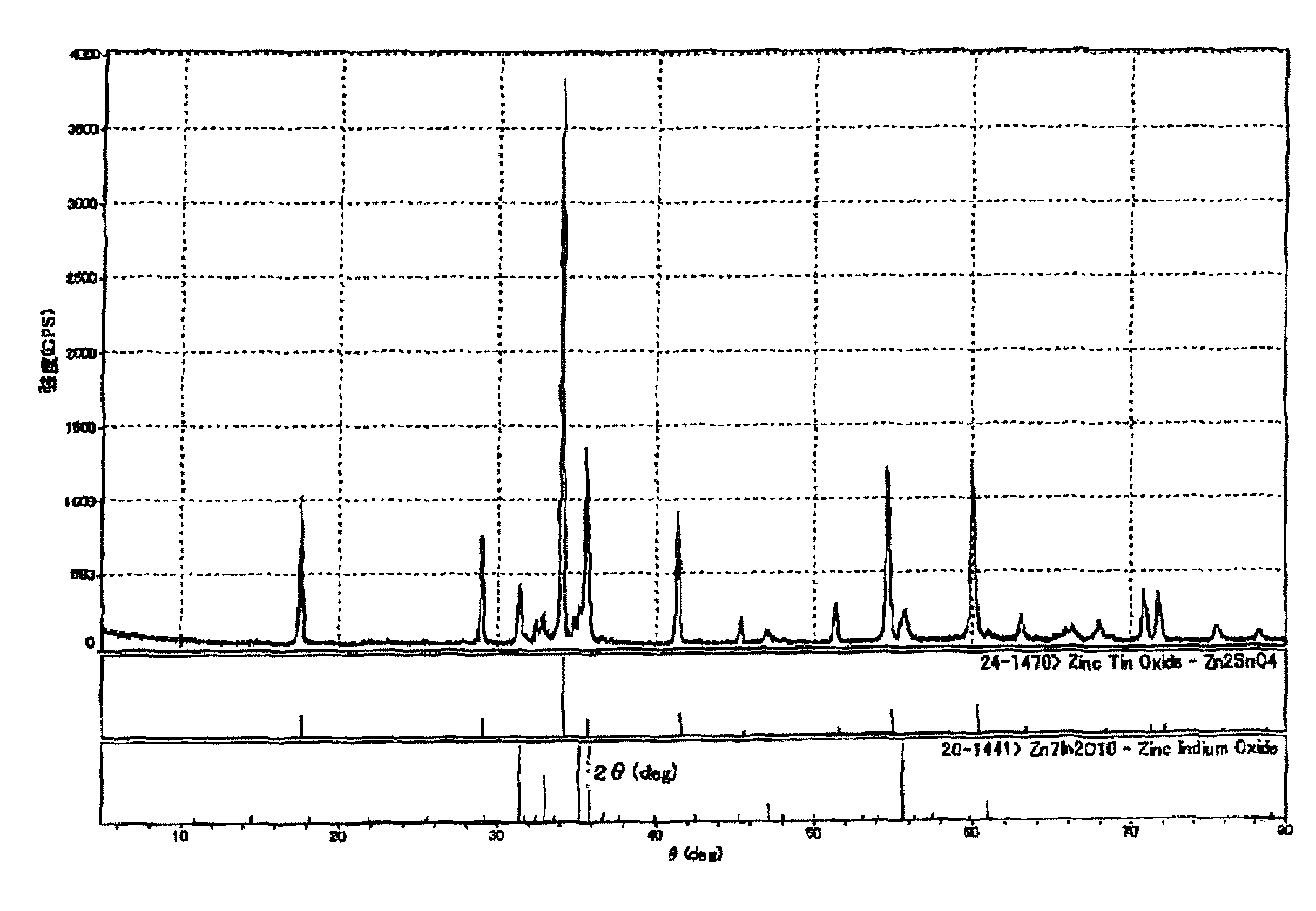
[0067]As raw materials, indium oxide with an average particle diameter of 1 μm and a purity of 4N, zinc oxide with an average particle diameter of 1 μm and a purity of 4N, and tin oxide with an average particle diameter of 1 μm and a purity of 4N were mixed at atomic ratios of In / (In+Sn+Zn)=0.16, Sn / (In+Sn+Zn)=0.20, and Zn / (In+Sn+Zn)=0.64. The mixture was supplied to a wet-type ball mill and pulverized for 20 hours to obtain a raw material fine powder.

[0068]The resulting mixture slurry was removed, filtered, dried and granulated. The granulated product was then molded by the cold isostatic pressing at a pressure of 294 MPa. The molded product was placed in a firing kiln, and fired at 1400° C. for 48 hours under an oxygen gas pressure, whereby a sintered body (target) was obtained. The heating rate was 50° C. / hour until the temperature reached 1,000° C. Between 1,000° C. and 1,400° C., the heating rate was 150° C. / hour. The cooling rate was 100° C. / ...


PUM

PropertyMeasurementUnit
temperatureaaaaaaaaaa
crystal grain diameteraaaaaaaaaa

Abstract

A sputtering target which is composed of a sintered body of an oxide containing indium, tin and zinc as main components; the atomic ratio of In / (In+Sn+Zn) being 0.10 to 0.35; the atomic ratio of Sn / (In+Sn+Zn) being 0.15 to 0.35; and the atomic ratio of Zn / (In+Sn+Zn) being 0.50 to 0.70; and containing a hexagonal layered compound shown by In2O3(ZnO)m, wherein m is an integer of 3 to 9, and a spinel structure compound shown by Zn2SnO4.

Description

TECHNICAL FIELD[0001]The invention relates to a sputtering target having a reduced indium content, a transparent conductive film, and a transparent electrode for touch panels.BACKGROUND[0002]In recent years, development of displays has been remarkable. Liquid crystal displays (LCD), electroluminescence displays (EL), field emission displays (FED), or the like are used as display devices for business machines such as personal computers and word processors, and display devices for control systems in factories. These displays have a sandwich structure in which a display device is held between transparent conductive oxides.[0003]A mainstream material for such a transparent conductive oxide is indium tin oxide (hereinafter occasionally abbreviated as “ITO”) prepared by a sputtering method, an ion plating method, or a vapor deposition method as described in Non-Patent Document 1.[0004]ITO is composed of indium oxide and tin oxide, possesses excellent transparency and conductivity, can be ...

Claims


Application Information

Patent Timeline
Patent Type & Authority Patents(United States)
IPC IPC(8): C04B35/453C23C14/34
CPCC04B35/453C23C14/3414C04B35/62645C04B35/64C23C14/086C04B35/457C04B2235/3284C04B2235/3286C04B2235/3293C04B2235/5436C04B2235/5445C04B2235/652C04B2235/6562C04B2235/6565C04B2235/6584C04B2235/763C04B2235/767C23C14/34
Inventor YANO, KOKIINOUE, KAZUYOSHITANAKA, NOBUOTANAKA, LEGAL REPRESENTATIVE, TOKIESHIMANE, YUKIO
Owner IDEMITSU KOSAN CO LTD
Why Eureka
Try Eureka