Use of F-based gate etch to passivate the high-k/metal gate stack for deep submicron transistor technologies

a technology of deep submicron transistors and gate etching, which is applied in the direction of semiconductor devices, basic electric elements, electric devices, etc., can solve the problems of significant high amount of bulk defects and interface states, and the introduction of high-k and metal gate materials in scaled cmos technologies (45 nm nodes and beyond) faces significant difficulties, so as to increase the lifetime and performance of semiconductor devices.

Active Publication Date: 2012-11-27
INTERUNIVERSITAIR MICRO ELECTRONICS CENT (IMEC VZW) +1
View PDF6 Cites 22 Cited by
  • Summary
  • Abstract
  • Description
  • Claims
  • Application Information

AI Technical Summary

Benefits of technology

[0007]According to preferred embodiments, a method is provided to increase the lifetime and performance of a semiconductor device comprising a high-k material such as HfO2 by incorporation of Fluorine in the high-k material and more specifically to incorporate or replace the Si—H and Hf—H bonds (especially at the interface of the silicon substrate and HfO2) by Si—F and Hf—F bonds.

Problems solved by technology

The introduction of high-k and metal gate materials in scaled CMOS technologies (45 nm node and beyond) faces significant difficulties due to severe threshold voltage instability and performance degradation of the devices.
These problems are related to the high amount of bulk defects and interface states in the high-k / metal gate stack.
In addition, preferential lateral re-oxidation of the gate dielectric is a significant problem, especially for short channel devices.
However, implanting Fluorine during the gate stack deposition may lead to uncontrolled oxide re-growth as described by Mogul et al (IEEE Trans.

Method used


Image

  • Use of F-based gate etch to passivate the high-k/metal gate stack for deep submicron transistor technologies
  • Use of F-based gate etch to passivate the high-k/metal gate stack for deep submicron transistor technologies
  • Use of F-based gate etch to passivate the high-k/metal gate stack for deep submicron transistor technologies

Examples


example 1

MuGFET Device Fabrication According to a Preferred Embodiment

[0131]MuGFET devices have been fabricated on standard [100] / [110] (top surface) SOI substrates with fin height Hfin=60 nm and fin widths down to 20 nm.

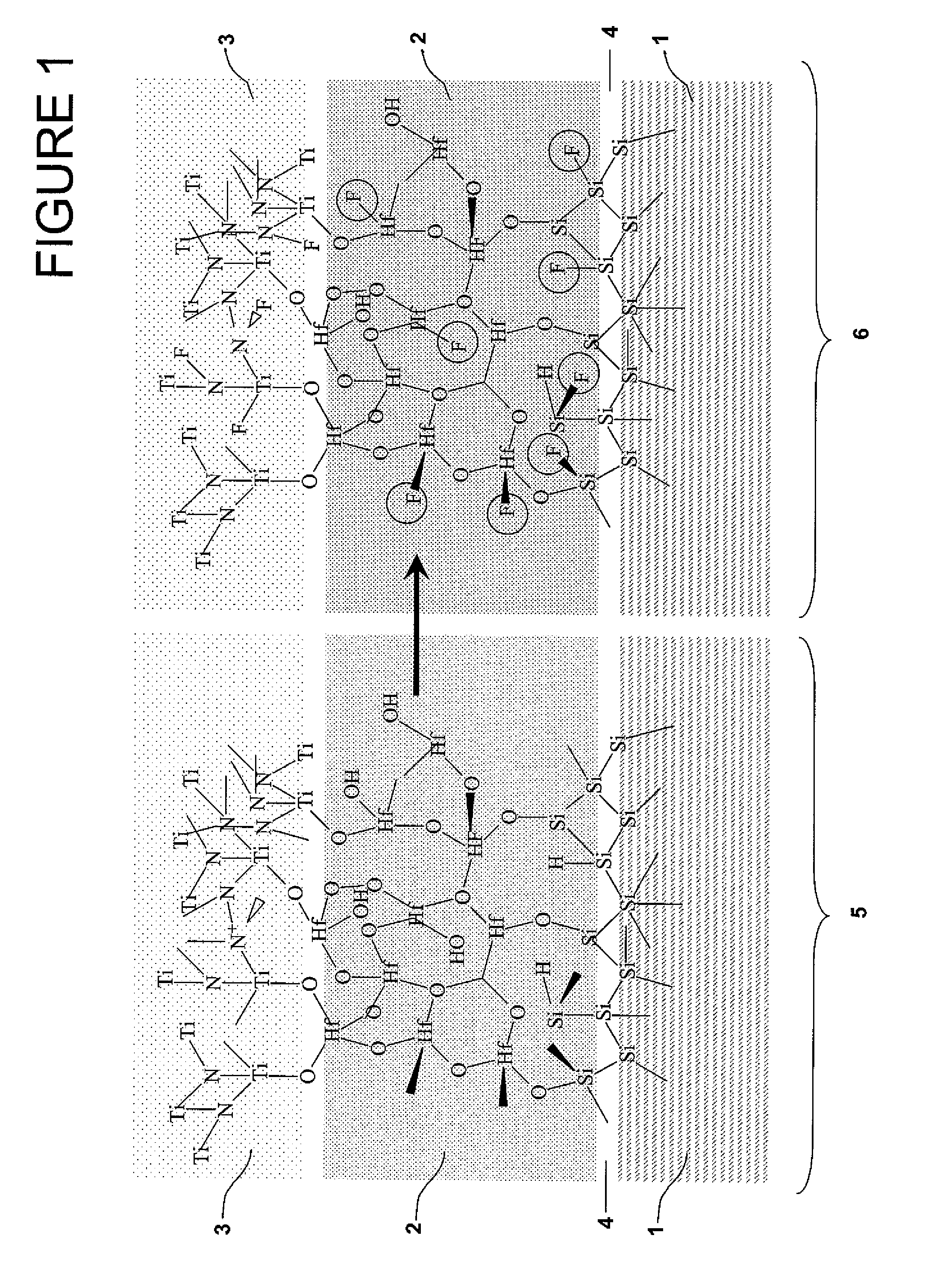
[0132]After fin patterning, the devices received a H2 anneal to smoothen the sidewalls and round the corners. The gate stack consists of a 5 nm ALD TiN layer on top of a 2 nm HfO2 / 1 nm SiO2 gate dielectric.

[0133]100 nm poly is used as a capping layer.

[0134]After gate stack deposition, an oxide hard mask (HM) is used to pattern the poly-silicon, stopping on the TiN layer.

[0135]For the TiN etch, BCl3 / Cl2 was used for the reference devices.

[0136]For the other devices, SF6 / O2 is used as gate-etch chemistry. The benefits of this chemistry are that it etches the TiN layer and at the same time introduces the necessary amount of F needed to passivate the interfaces of the high-k dielectric.

[0137]This method was demonstrated both for planar and MuGFET devices.

[0138]After gate pattern...

example 2

Gate Etch Processing and Transistor Performance

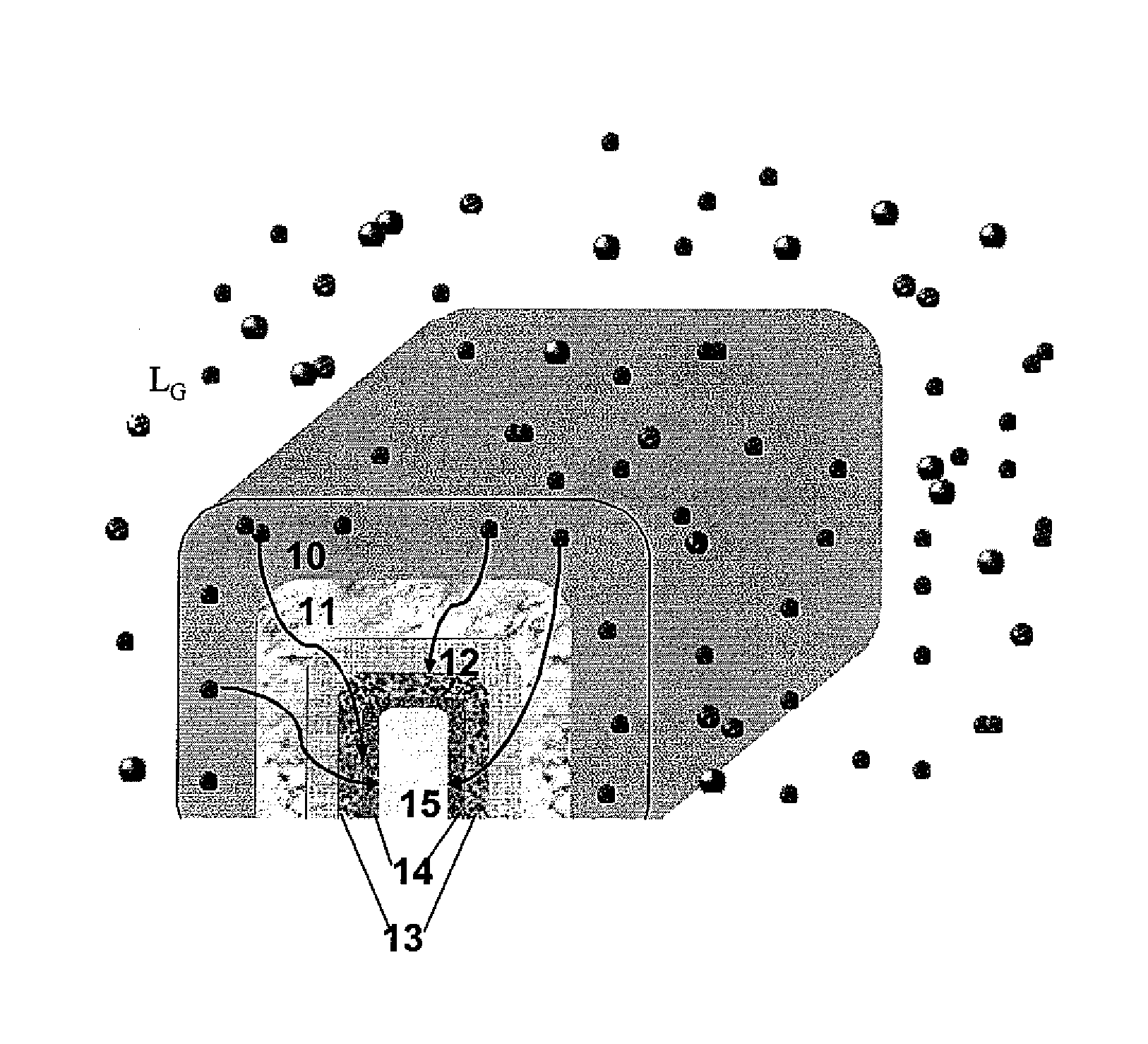
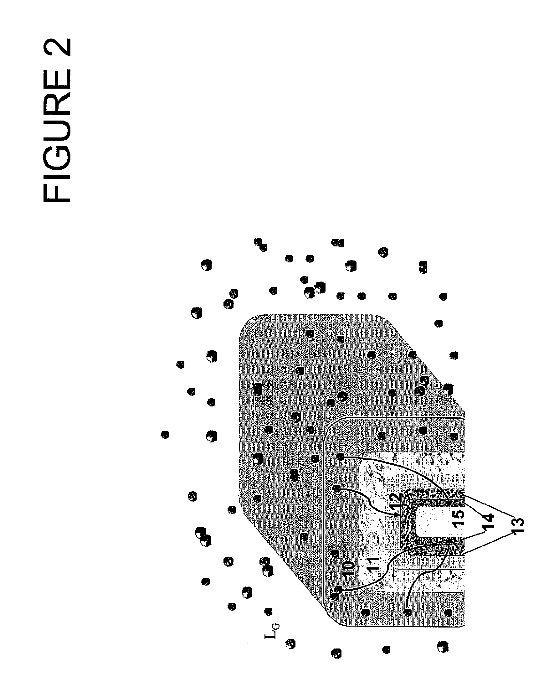
[0144]The metal gate etch processing is schematically depicted shown in FIG. 2. It is an isotropic etch and as consequence it has the same impact on all sides of the device.

[0145]During the TiN etch, F diffuses and accumulates in the hard mask (HM).

[0146]The thermal budget of the subsequent SEG step (750-810° C.) assists further diffusion of the accumulated F towards the dielectric interfaces. It also provides the necessary activation energy for passivating the interface states and / or for substituting the H atoms in the existing Si—H / Hf—H weaker bonds.

[0147]FIG. 3 shows the nFET and pFET saturation Vth versus gate length (LG).

[0148]An anomalous Vth behavior is seen for the reference devices (using no SF6 chemistry during the metal gate etch), a roll-up for nMOS and enhanced roll-off for pMOS). This behavior is typically attributed to process damage generated at the gate edges during device fabrication.

[0149]The SF6 / O2 devices do not exh...

example 3

Reliability Results in Devices Having Fluorine Incorporated in the Gate Dielectric

[0153]Interrupted stress (0.5 s delay) BTI measurements were performed at stress VG in the |1-2.2| V range and temperatures from 125 to 175° C.

[0154]The studied MuGFET devices (Wfin≦Hfin) have dimensions Wfin=20 nm, Hfin=60 nm, Nfins=30 (various LG). Planar devices (Wfin>>Hfin) have LG=Wfin=1 μm.

[0155]Si—F and Hf—F bonds have higher dissociation energies than Si—H and Hf—H, and are not broken during stress conditions similar or higher to typical operating conditions, such as temperature of 125-175° C. and electric fields (Eox) of 3-8 MV / cm (see FIG. 6).

[0156]FIG. 7 shows that the Eox, distribution in MuGFET and planar SOI devices is similar. As a consequence, the same Eox, evaluation method can be used in both cases.

[0157]FIG. 8 shows the NBTI lifetime improvement for devices having used a SF6 / O2 etch chemistry during metal gate etch (and additional selective epitaxial growth (SEG) as described above a...


PUM


Abstract

A new, effective and cost-efficient method of introducing Fluorine into Hf-based dielectric gate stacks of planar or multi-gate devices (MuGFET), resulting in a significant improvement in both Negative and Positive Bias Temperature Instabilities (NBTI and PBTI) is provided. The new method uses an SF6 based metal gate etch chemistry for the introduction of Fluorine, which after a thermal budget within the standard process flow, results in excellent F passivation of the interfaces. A key advantage of the method is that it uses the metal gate etch for F introduction, requiring no extra implantations or treatments. In addition to the significant BTI improvement with the novel method, a better Vth control and increased drive current on MuGFET devices is achieved.

Description

CROSS-REFERENCE TO RELATED APPLICATIONS[0001]This application claims the benefit under 35 U.S.C. §119(e) of U.S. provisional application Ser. No. U.S. 60 / 879,704 filed Jan. 10, 2007, the disclosure of which is hereby expressly incorporated by reference in its entirety and is hereby expressly made a portion of this application.FIELD OF THE INVENTION[0002]The preferred embodiments are related to the field of gate patterning in planar and multiple-gate devices. More specifically the preferred embodiments are related to the simultaneous incorporation of Fluorine into the gate stack during the patterning of said gate stack. The preferred embodiments are further related to the creation of semiconductor devices with increased lifetime and significant Bias Temperature instability (BTI) improvement. The preferred embodiments are especially beneficial for short channel devices.BACKGROUND OF THE INVENTION[0003]The introduction of high-k and metal gate materials in scaled CMOS technologies (45 ...

Claims


Application Information

Patent Timeline
Patent Type & Authority Patents(United States)
IPC IPC(8): H01L29/423H01L21/302
CPCH01L21/28079H01L21/28088H01L21/28097H01L21/28176H01L21/28247H01L21/3105H01L29/4958H01L29/4966H01L29/4975H01L29/517H01L29/66795H01L21/32136H01L29/785
Inventor COLLAERT, NADINEZIMMERMAN, PAULDEMAND, MARCBOULLART, WERNERSHICKOVA, ADELINA K.
Owner INTERUNIVERSITAIR MICRO ELECTRONICS CENT (IMEC VZW)
Why Eureka
Try Eureka