
Software reconfigurable digital phase lock loop architecture

a software and phase lock technology, applied in the field of data communication, can solve the problems of difficult one design to support multi-standard wireless applications, many time-consuming steps, and limited reconfigurability of conventional adpll circuits, and achieve the effect of reducing the per cycle current transient and reducing the number of spurs

Active Publication Date: 2012-11-27
TEXAS INSTR INC
View PDF5 Cites 26 Cited by
  • Summary
  • Abstract
  • Description
  • Claims
  • Application Information

AI Technical Summary

Benefits of technology

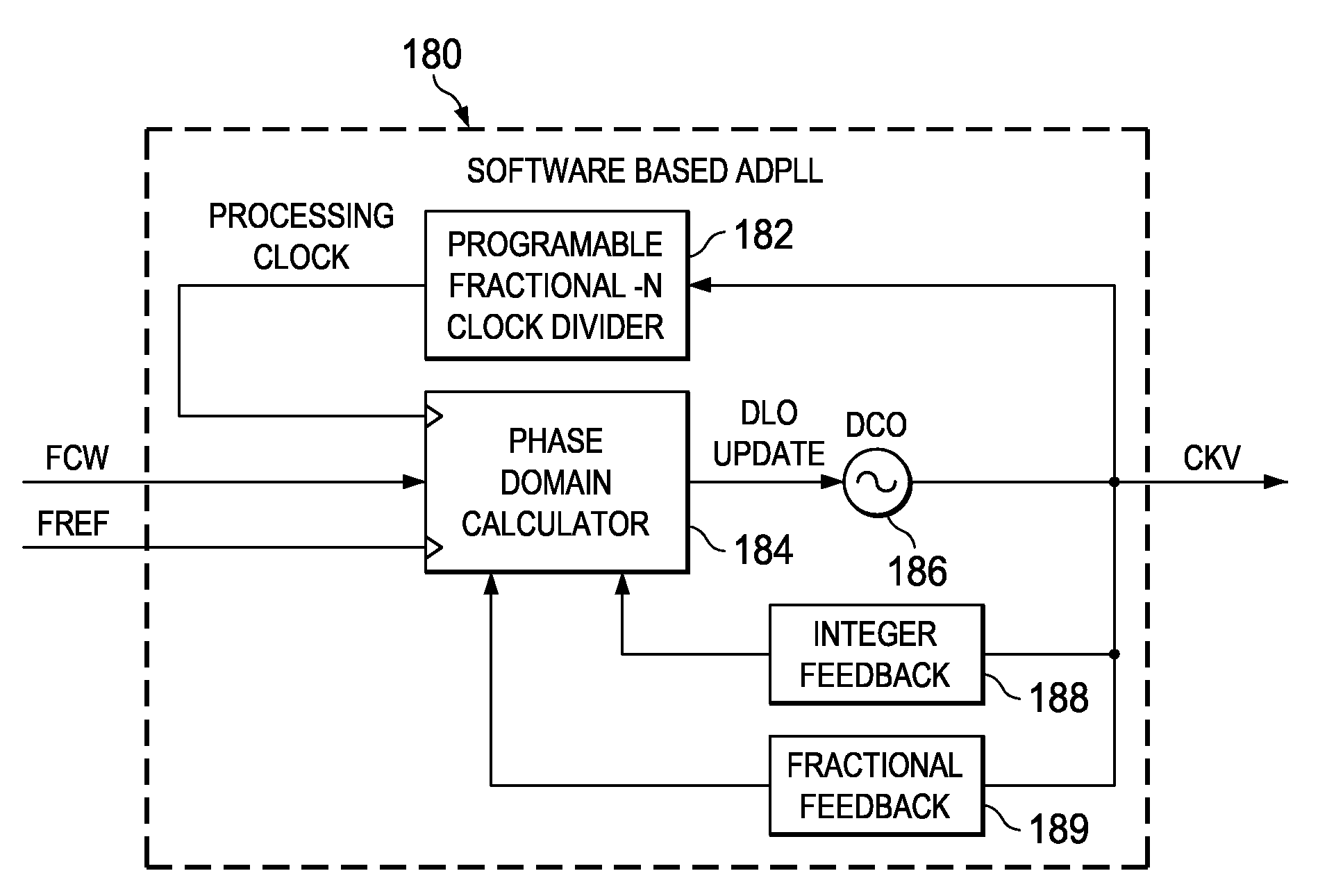
[0017]In one embodiment, the instruction set is implemented in microcode that is stored in volatile or non-volatile memory. Thus, the ASIP can easily be reconfigured to implement customized designs for different applications, such as multiple cellular standards, including GSM, GPRS, EDGE, WCDMA, Bluetooth, WiFi, etc., as well as wireless data network standards, including Bluetooth, WiFi, WiMAX, etc. The ASIP can be configured on the fly to handle the different RF frequency and performance requirements of each communication standard. The software based PLL of the present invention provides the flexibility for a more unified design that fits different applications.
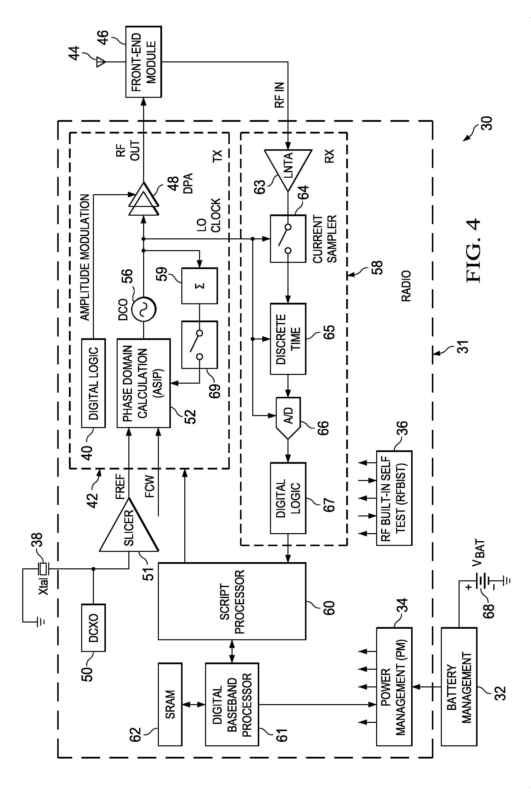
[0018]In a second embodiment, the phase locked loop task is partitioned into a plurality of atomic operations. The ASIP is adapted to spread the computation of the atomic operations out over and completed within an entire PLL reference clock period. Each computation being performed at a much higher processor clock frequency than the PLL reference clock rate. This functions to significantly reduce the per cycle current transient generated by the computations. Further, the frequency content of the current transients is at the higher processor clock frequency. This results in a significant reduction in spurs within sensitive portions of the output spectrum.
[0020]Advantages of the software reconfigurable phase locked loop of the present invention include the following. Firstly, the invention enables all phase domain calculations to be performed within one reference clock cycle due to the use of the reconfigurable calculation unit optimized for performing PLL calculations serially at high frequency. Secondly, defining the ASIP instruction set in microcode stored in volatile or non-volatile memory makes it inherently software reconfigurable, permitting the microcode to be replaced without changing any lithography masks. The enables easier silicon debugging and multi-standard radio support.
[0022]Fourthly, the invention enables a significant reduction of RF spurs in the sensitive frequency bands of a radio by changing the frequency of the switching logic gates. Prior art solutions perform PLL computations at relatively low rates, e.g., FREF of 26-38.8 MHz. The resulting switching current transients are mixed with the carrier and appear as frequency spurs at sensitive radio frequency bands. Considering GSM, for example, the most sensitive RX band is approximately 20 to 80 MHz away from the carrier. The invention performs the bulk of computations at oversampled rates, resulting in spurs outside sensitive regions. The amount of oversampling can be controlled (e.g., increased or decreased) to provide any desired frequency planning by changing the frequency of the processing clock. Fifthly, reduction in silicon area provided by the invention enables power routing and decoupling capacitance requirements to be relaxed.

Problems solved by technology

Conventional ADPLL circuits, however, are implemented as purely fixed hardware based (or hardwired) with very limited reconfigurability.
It is thus difficult for one design to support multi-standard wireless applications, e.g., GSM, GPRS, EDGE, WCDMA, etc. as well as wireless data networks, such as Bluetooth, WiFi and WiMAX.
Any modification requiring logic and interconnect change results in numerous time consuming steps within the ASIC creation process (i.e. timing closure, physical design, etc.) typically requiring significant engineering resources and months of delay to launch a product.
In addition, once the silicon is manufactured, any change to the ADPLL architecture makes an even costlier impact, making such changes virtually impractical.
The interconnections in a hardwired design having a large area will significantly slow the circuit speed while adding a significant silicon area overhead.
These disturbances at the system clock rate have strong sub-harmonics that are upconverted into sensitive areas of the RF spectrum, resulting in unacceptable RF spurs.

Method used


Image

  • Software reconfigurable digital phase lock loop architecture
  • Software reconfigurable digital phase lock loop architecture
  • Software reconfigurable digital phase lock loop architecture

Examples


Embodiment Construction

Notation Used Throughout

[0060]The following notation is used throughout this document.

[0061]

TermDefinitionACAlternating CurrentACLAsynchronous Connectionless LinkACWAmplitude Control WordADCAnalog to Digital ConverterADPLLAll Digital Phase Locked LoopALUArithmetic Logic UnitAMAmplitude ModulationASICApplication Specific Integrated CircuitASIPApplication Specific Instruction-set ProcessorAVIAudio Video InterfaceAWSAdvanced Wireless ServicesBISTBuilt-In Self TestBMPWindows BitmapBPFBand Pass FilterCMOSComplementary Metal Oxide SemiconductorCPUCentral Processing UnitCUControl UnitCWContinuous WaveDACDigital to Analog ConverterdBDecibelDBBDigital BasebandDCDirect CurrentDCODigitally Controlled OscillatorDCXODigitally Controlled Crystal OscillatorDPADigitally Controlled Power AmplifierDRACDigital to RF Amplitude ConversionDRPDigital RF Processor or Digital Radio ProcessorDSLDigital Subscriber LineDSPDigital Signal ProcessorEDGEEnhanced Data Rates for GSM EvolutionEDREnhanced Data RateEEP...


PUM


Abstract

A novel and useful apparatus for and method of software based phase locked loop (PLL). The software based PLL incorporates a reconfigurable calculation unit (RCU) that is optimized and programmed to sequentially perform all the atomic operations of a PLL or any other desired task in a time sharing manner. An application specific instruction-set processor (ASIP) incorporating the RCU includes an instruction set whose instructions are optimized to perform the atomic operations of a PLL. The RCU is clocked at a fast enough processor clock rate to insure that all PLL atomic operations are performed within a single PLL reference clock cycle.

Description

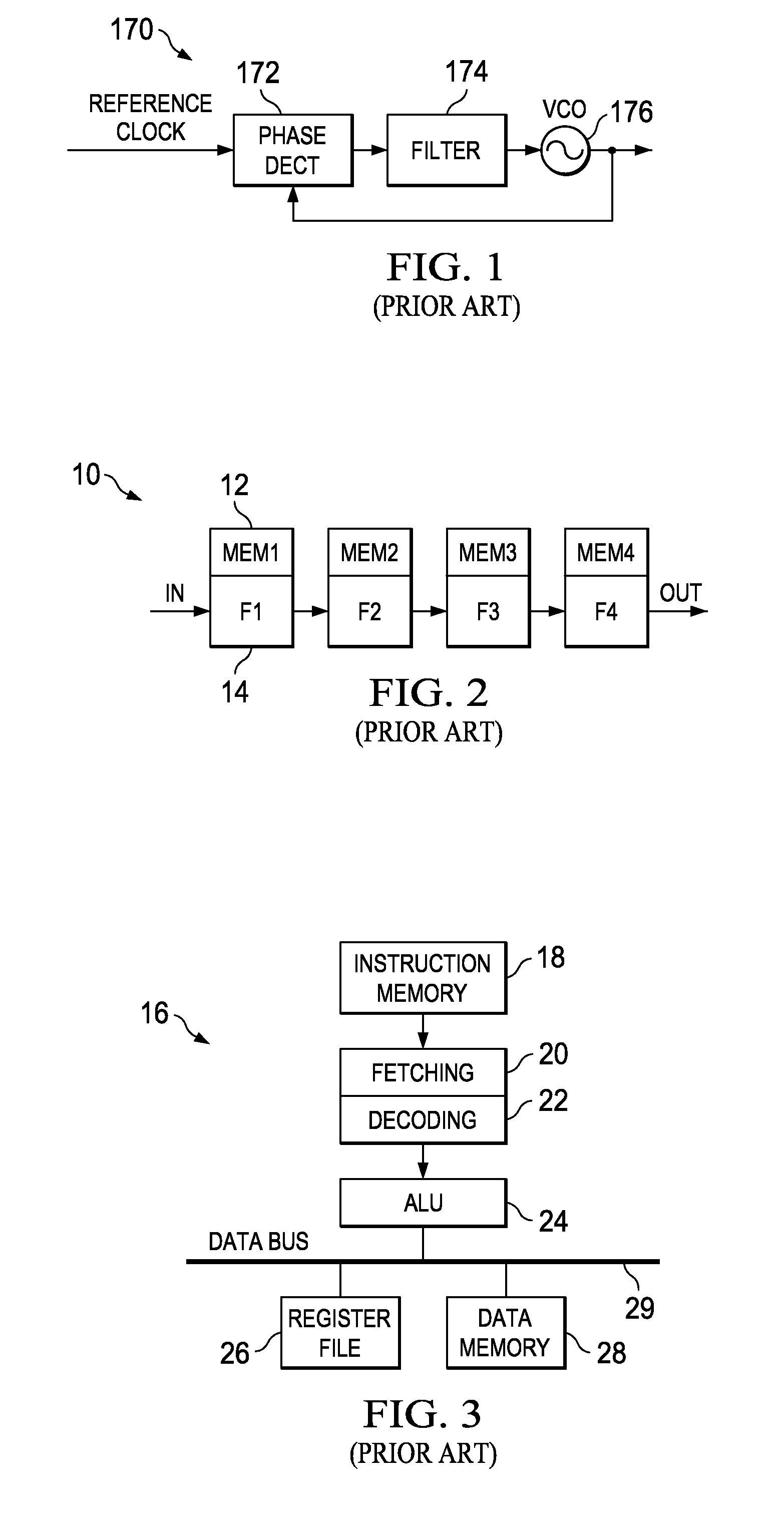
REFERENCE TO PRIORITY APPLICATION[0001]This application claims priority to U.S. Provisional Application Ser. No. 60 / 825,838, filed Sep. 15, 2006, entitled “Software Reconfigurable All Digital Phase Lock Loop”, incorporated herein by reference in its entirety.FIELD OF THE INVENTION[0002]The present invention relates to the field of data communications and more particularly relates to a software reconfigurable all digital phase locked loop (ADPLL) architecture and application specific instruction-set processor related thereto.BACKGROUND OF THE INVENTION[0003]Phase locked loop (PLL) circuits are well known in the art. A block diagram illustrating an example prior art phase locked look (PLL) circuit is shown in FIG. 1. The typical PLL circuit, generally referenced 170, comprises phase detector 172, loop filter or low pass filter (LPF) 174 and voltage controlled oscillator (VCO) 176.[0004]In operation, a frequency reference clock signal, often derived from a crystal oscillator, is input ...

Claims


Application Information

Patent Timeline
Patent Type & Authority Patents(United States)
IPC IPC(8): G06F17/10
CPCG06F9/30032G06F9/30181H03L7/1976G06F7/605H04W56/003G06F17/10H03L7/0992H03L7/1974H04B1/04G06F9/30014H03L2207/50
Inventor STASZEWSKI, ROMANSTASZEWSKI, ROBERT B.SHI, FUQIANG
Owner TEXAS INSTR INC
Learn More