Magnetic tunnel junction for MRAM applications

a technology of magnetic tunnel junction and mram, applied in the direction of magnets, instruments, inductance/transformer/magnet manufacture, etc., can solve the problems of poor writing margin, inability to directly apply structure in mram, deformation in one or more other parameters, etc., to improve reading margin, improve mr ratio, and not degrade writing margin

Active Publication Date: 2013-07-23
TAIWAN SEMICON MFG CO LTD
View PDF9 Cites 50 Cited by
  • Summary
  • Abstract
  • Description
  • Claims
  • Application Information

AI Technical Summary

Benefits of technology

[0014]One objective of the present invention is to provide a pinned layer / tunnel barrier / free layer stack for a MTJ element that improves reading margin and improves MR ratio but does not degrade writing margin, or increase the number of shorts, or increase the number of unswitched bits at a given bit line current compared with the prior art.
[0015]A second objective of the present invention is to achieve the improved performance of the first objective without introducing new materials or processes that would increase the cost of fabricating a MTJ element.
[0018]A composite free layer adjoins a surface of the tunnel barrier layer and preferably has a Fe / NiFeX or CoFe / Fe / NiFeX configuration where X is one of Hf, Zr, Nb, Ta, or Mg with a content of about 5 to 30 atomic %. For example, a CoFe / Fe / NiFeHf composite free layer is especially suited to realize the objectives and advantages of the present invention. Preferably, the CoFe free layer has an Fe content of 60 to 90 atomic %, and the NiFeHf layer should be in the range of 20 to 40 Angstroms thick to provide the full advantage of a reduced number of shorted bits and a substantially lower bit switching current. A capping layer such as Ru or Ru / Ta / Ru is the uppermost layer in the MTJ stack and contacts the NiFeHf layer or NiFeX layer.

Problems solved by technology

Typically, an improvement in one property leads to a degradation in one or more other parameters.
In addition, recent developments show that a MgO / CoFeB tunnel barrier / free layer configuration exhibits very high MR ratio (>200%) but this structure could not be directly applied in MRAM because a MTJ with a CoFeB free layer shows very poor writing margin (wide bit-to-bit switching current) due to its high anisotropy energy.
Moreover, a high switch current is needed because of high coercivity associated with a CoFeB free layer.

Method used


Image

  • Magnetic tunnel junction for MRAM applications
  • Magnetic tunnel junction for MRAM applications
  • Magnetic tunnel junction for MRAM applications

Examples


first embodiment

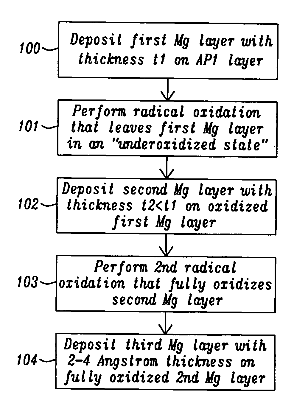
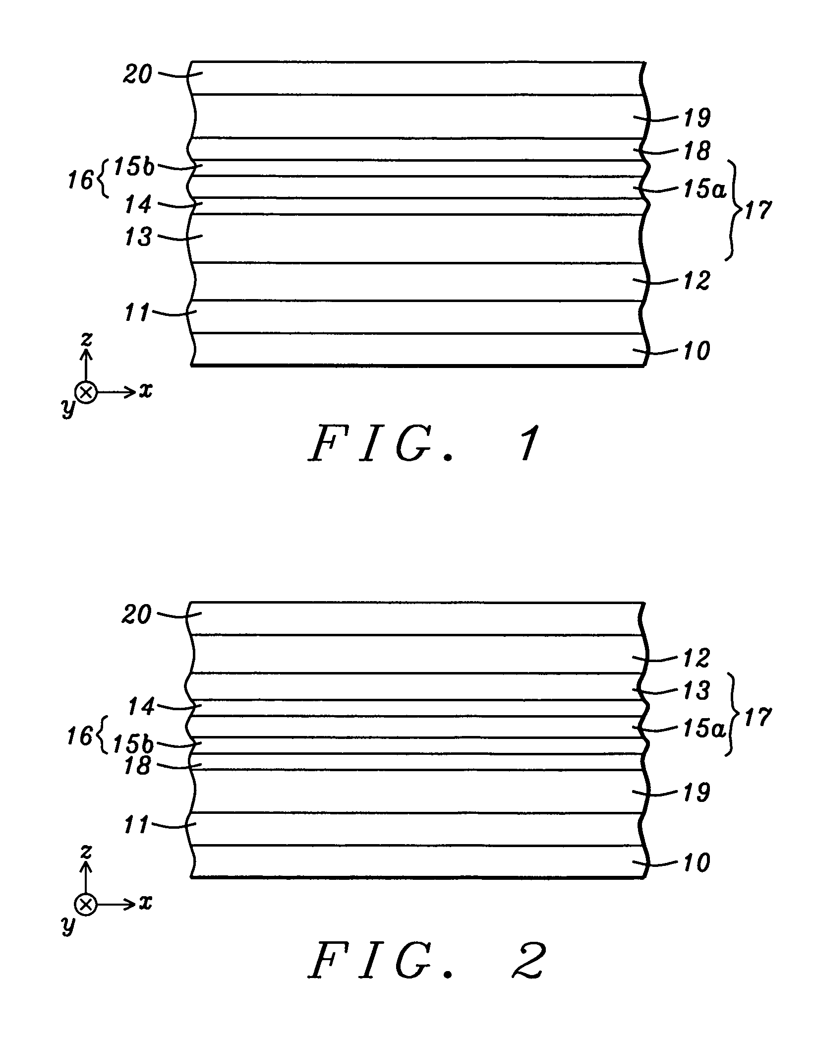
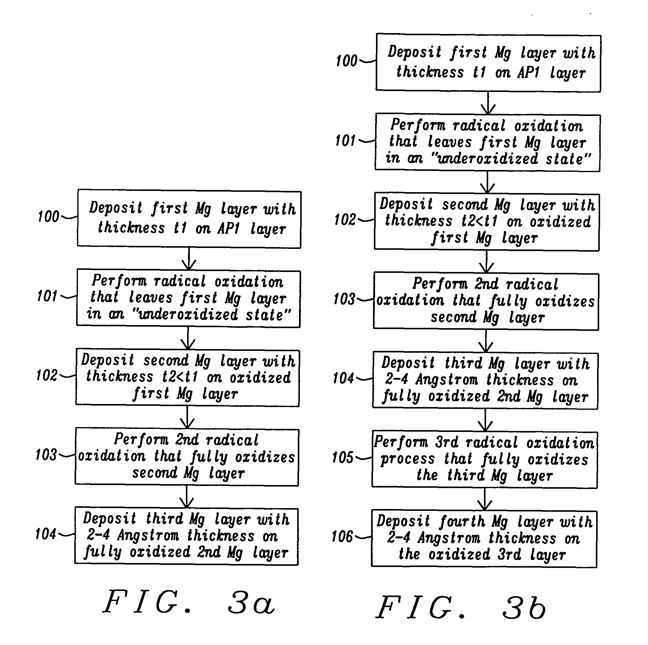
[0030]Referring to FIG. 1, a MTJ structure is illustrated according to the present invention. The substrate 10 may be a bottom conductor layer, for example, also known as a bottom electrode and having a thickness in the z-axis direction and with a top surface in the x,y plane. A MTJ stack of layers is now formed on the substrate 10. It should be understood that all layers in the MTJ stack may be formed in the same process tool such as an Anelva C-7100 thin film sputtering system or the like which typically includes three physical vapor deposition (PVD) chambers, an oxidation chamber, and a sputter etching chamber. At least one of the PVD chambers is capable of co-sputtering using two or more targets. Typically, the sputter deposition process involves an argon sputter gas and the targets are made of metal or alloys to be deposited on a substrate. All MTJ layers may be formed after a single pump down of the sputter system to enhance throughput.

[0031]In the exemplary embodiment depicti...

second embodiment

[0048]According to the present invention as depicted in FIG. 2, the free layer 19 as described in the bottom spin valve embodiments may be formed in a top spin valve configuration. For example, the MTJ stack may be fabricated by sequentially forming a seed layer 11, composite free layer 19, tunnel barrier 18, SAF pinned layer 17, AFM layer 12, and capping layer 20 on substrate 10. In this case, free layer 19 may have a FL2 / FL1 (NiFeX / Fe) or a FL3 / FL2 / FL1 (NiFeX / Fe / CoFe) configuration wherein the NiFeX layer is the bottom layer in the free layer stack and contacts a top surface of seed layer 11. Thus, the uppermost FL1 layer interfaces with the tunnel barrier 18 to produce a high MR ratio. The properties and thicknesses of the aforementioned layers are retained from the previous embodiments. Note that the SAF pinned layer 17 has an AP1 / coupling / AP2 configuration wherein the AP1 layer 16 contacts a top surface of the tunnel barrier layer and the AP2 layer 13 contacts a bottom surface ...


PUM


Abstract

Reading margin is improved in a MTJ designed for MRAM applications by employing a pinned layer with an AP2 / Ru / AP1 configuration wherein the AP1 layer is a CoFeB / CoFe composite and by forming a MgO tunnel barrier adjacent to the CoFe AP1 layer by a sequence that involves depositing and oxidizing a first Mg layer with a radical oxidation (ROX) process, depositing and oxidizing a second Mg layer with a ROX method, and depositing a third Mg layer on the oxidized second Mg layer. The third Mg layer becomes oxidized during a subsequent anneal. MTJ performance may be further improved by selecting a composite free layer having a Fe / NiFeHf or CoFe / Fe / NiFeHf configuration where the NiFeHf layer adjoins a capping layer in a bottom spin valve configuration. As a result, read margin is optimized simultaneously with improved MR ratio, a reduction in bit line switching current, and a lower number of shorted bits.

Description

RELATED PATENT APPLICATIONS[0001]This application is related to the following: Ser. No. 12 / 930,877; filing date Jan. 19, 2011; and Ser. No. 13 / 068,222, filing date May 5, 2011; all assigned to a common assignee and herein incorporated by reference in their entirety.FIELD OF THE INVENTION[0002]The invention relates to a high performance Magnetic Tunneling Junction (MTJ) element and, in particular, to a pinned layer / tunnel barrier / free layer stack that lowers bit to bit resistance variation (Rp_cov) thereby improving reading margin without compromising other MTJ properties such as writing margin, MR ratio, and number of shorted bits.BACKGROUND OF THE INVENTION[0003]Magnetoresistive Random Access Memory (MRAM), based on the integration of silicon CMOS with MTJ technology, is a major emerging technology that is highly competitive with existing semiconductor memories such as SRAM, DRAM, Flash, etc. A MRAM device is generally comprised of an array of parallel first conductive lines on a h...

Claims


Application Information

Patent Timeline
Patent Type & Authority Patents(United States)
IPC IPC(8): H01L29/82H01L29/88G11C11/02
CPCH01L43/12H01F41/307B82Y40/00H01F10/3295H01L43/10H01F10/3272H10N50/01H10N50/85
Inventor CAO, WEIKULA, WITOLDTORNG, CHYU-JIUH
Owner TAIWAN SEMICON MFG CO LTD
Why Eureka
Try Eureka