Dye-sensitized solar cell

a solar cell, dye-sensitive technology, applied in the manufacture of final products, electrochemical generators, pv power plants, etc., can solve the problems of increasing and achieve the effect of reducing the manufacturing cost of the cell and superior optical absorption efficiency

Inactive Publication Date: 2013-09-10
NIPPON STEEL CHEMICAL CO LTD +1
View PDF12 Cites 9 Cited by
  • Summary
  • Abstract
  • Description
  • Claims
  • Application Information

AI Technical Summary

Benefits of technology

[0029]A dye-sensitized solar cell according to the present invention comprises an anode substrate, a first dye-carrying porous oxide semiconductor layer held by the anode substrate, a first electrolytic solution layer, and a cathode substrate, arranged in order from an optical incidence side, and further includes a redox catalyst layer, a porous support layer, a second dye-carrying porous oxide semiconductor layer, and a second electrolytic solution layer, or further includes a porous conductive metal support layer, a second dye-carrying porous oxide semiconductor layer, and a second electrolytic solution layer. Consequently, the dye-sensitized solar cell is superior in optical absorption efficiency, and does not necessarily require an expensive transparent conductive film or need not use the film in large amounts. Thus, the manufacturing cost of the cell can be reduced.

Problems solved by technology

However, every solar cell of the above-described related arts involves, for example, a further improvement in optical absorption efficiency, an increase in the manufacturing cost of the cell caused by using many expensive transparent conductive films for reasons of a cell structure, or disadvantages when the cell is increased in size.

Method used


Image

  • Dye-sensitized solar cell
  • Dye-sensitized solar cell
  • Dye-sensitized solar cell

Examples


example 1

Practical Example 1

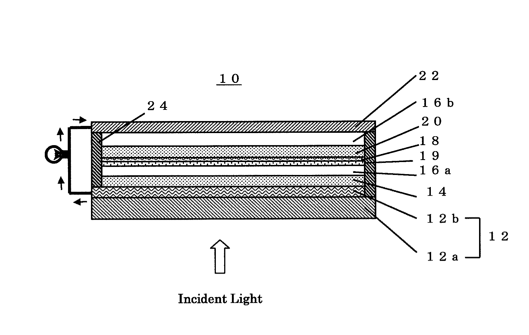
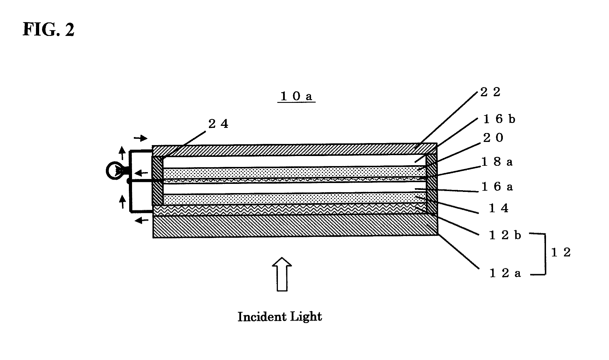
[0068]An FTO film (surface resistance: 10 Ω / sq) was formed on a transparent glass substrate, and titania paste was coated on the FTO film and dried at 450° C. for 30 minutes, thereby fabricating a 2 μm-thick porous titania layer. The above-described first dye (Dye 2) was adsorbed to this porous titania layer to fabricate a first electrode. On the other hand, titanium was film-formed by sputtering on a stainless mesh substrate (25 μm in thickness) including a mesh 20 μm in diameter. Thereafter, titanium was further film-formed using arc plasma while introducing oxygen, thereby fabricating a surface-protected stainless mesh structure. Titania paste was coated on the mesh structure and dried at 450° C. for 30 minutes, thereby fabricating a 2 μm-thick porous titania layer. After platinum was sputtered on a surface of the mesh structure on the side thereof on which the porous titania layer was not provided, the above-described second dye (Dye 2) was adsorbed to this ti...

example 2

Practical Example 2

[0070]An FTO film (surface resistance: 10 / sq) was formed on a transparent glass substrate, and titania paste was coated on the FTO film and dried at 450° C. for 30 minutes, thereby fabricating a 2 μm-thick porous titania layer. The first dye was adsorbed to this titania layer to fabricate a first electrode. On the other hand, titanium was film-formed by sputtering on a stainless mesh substrate (25 μm in thickness) including a mesh 20 μm in diameter. Thereafter, titanium was further film-formed using arc plasma while introducing oxygen, thereby fabricating a surface-protected stainless mesh structure. Titania paste was coated on the mesh structure and dried at 450° C. for 30 minutes, thereby fabricating a 2 μm-thick porous titania layer. The second dye was adsorbed to this titania layer, thereby fabricating a second electrode. For an electrolytic solution, a gel electrolytic solution prepared by impregnating a porous PTFE (polytetrafluoroethylene) film (50 μm in t...

reference example 1

[0072]Titania paste was coated on a stainless mesh substrate (25 μm in thickness) including a mesh 20μm in diameter and dried at 450° C. for 30 minutes, thereby fabricating a porous titania layer. This coating and drying of the titania paste was repeated until the thickness of the porous titania layer reached a predetermined thickness, thereby finally fabricating a 10 μm-thick porous titania layer. A dye (D-149 made by Mitsubishi Paper Mills Limited) having the chemical structure of the dye 3 shown in FIG. 6 was adsorbed to this titania layer to fabricate a second electrode. For an electrolytic solution, a gel electrolytic solution prepared by impregnating a porous PTFE (polytetrafluoroethylene) film (35 μm in thickness and 71% in porosity) with an electrolytic solution was used. A counter electrode was fabricated by sputtering platinum on titanium. The titania layer side of the porous titania layer fabricated as described above and the platinum side of the counter electrode were la...


PUM


Abstract

There is provided a tandem-type dye-sensitized solar cell having a novel structure whereby optical absorption efficiency is improved and which can be manufactured at low cost.A dye-sensitized solar cell 10 comprises an anode substrate 12, a first dye-carrying porous oxide semiconductor layer 14, an electrolytic solution layer 16a, a porous support layer 18, a second dye-carrying porous oxide semiconductor layer 20, an electrolytic solution layer 16b, and a cathode substrate 22, arranged in order from an optical incidence side. The porous support layer 18 supports an iodine redox catalyst layer 19. Electrons derived by a conductor from a conductor layer 12b are introduced to the cathode substrate 22, thereby configuring, for example, a battery circuit for lighting purposes.

Description

TECHNICAL FIELD[0001]The present invention relates to a so-called tandem-type dye-sensitized solar cell in which two porous oxide semiconductor layers each carrying a dye are provided in series with respect to a traveling direction of light.BACKGROUND ART[0002]The dye-sensitized solar cell is called a wet solar cell, a Graetzel cell, or the like, and has an electrochemical cell structure as typified by an iodine solution without using a silicon semiconductor. Specifically, the dye-sensitized solar cell has a simple structure in which an iodine solution or the like is disposed as an electrolyte solution between a porous semiconductor layer (porous oxide semiconductor layer), such as a titania layer, formed by baking titanium dioxide powder or the like onto a transparent conductive glass plate (a transparent substrate having a transparent conductive film laminated thereon and serving as an anode substrate) and making a dye adsorbed onto the baked powder, and a counter electrode compos...

Claims


Application Information

Patent Timeline
Patent Type & Authority Patents(United States)
IPC IPC(8): H01L31/0248H01L31/0216
CPCH01G9/2072H01G9/2031H01G9/2059Y02P70/521H01M14/005Y02E10/542H01L51/0064Y02P70/50H10K85/652H01L31/04
Inventor HAYASE, SHUZIYAMAGUCHI, YOSHIHIRO
Owner NIPPON STEEL CHEMICAL CO LTD
Why Eureka
Try Eureka