
Compositions and methods for modulation of nanostructure energy levels

a technology of energy level and nanostructure, applied in the field of nanotechnology, can solve the problems of large and/or disordered and/or low density packing nanoparticles, high cost (high temperature, high vacuum), and the thickness of the nanostructure generated by these and other standard core-shell synthetic techniques is not thick enough to confine a charge in the core. , to achieve the effect of increasing the level of the highest occupied molecular orbital (homo) and reducing the homo level

Active Publication Date: 2013-10-22
WODEN TECH INC
View PDF127 Cites 130 Cited by
  • Summary
  • Abstract
  • Description
  • Claims
  • Application Information

AI Technical Summary

Benefits of technology

This patent describes how to make a connection between a nanostructure, like a quantum dot, and a ligand composition. This connection can affect the energy levels of the nanostructure and the ligand, which can help to reduce charge diffusion among the nanostructures. The ligand composition can have different energy levels depending on its molecular structure. This method can be useful for making use of quantum dots in applications where there needs to be precise control over electron transfer or electric current.

Problems solved by technology

These methods typically yield large and / or disordered and / or low density packing nanoparticles, and require high cost (high temperature, high vacuum) processing steps.
However, nanostructures generated by these and other standard core-shell synthetic techniques typically do not have a thick enough shell to confine a charge in the core to enough degree to prevent charge diffusion to other nanostructures placed within a few nanometers of the first nanostructure.
While useful for enhancing solubility and facilitating manipulation of the nanostructures during synthesis, the organic contaminants are avidly associated with the nanostructure surface, thus inhibiting further manipulation and / or integration of the newly synthesized nanostructure into devices and end applications.
Even if these CdSe:ZnS constructs could be prepared having diameters allowing for high density packing (e.g., about 1×10¹² / cm2 or greater), the ZnS shell would not provide enough quantum confinement for efficient use of the nanostructures in microelectronic and photonic devices, including, but not limited to, memory or charge storage devices.

Method used


Image

  • Compositions and methods for modulation of nanostructure energy levels
  • Compositions and methods for modulation of nanostructure energy levels
  • Compositions and methods for modulation of nanostructure energy levels

Examples


example 1

Preparation of Closely Packed Nanostructure Monolayers

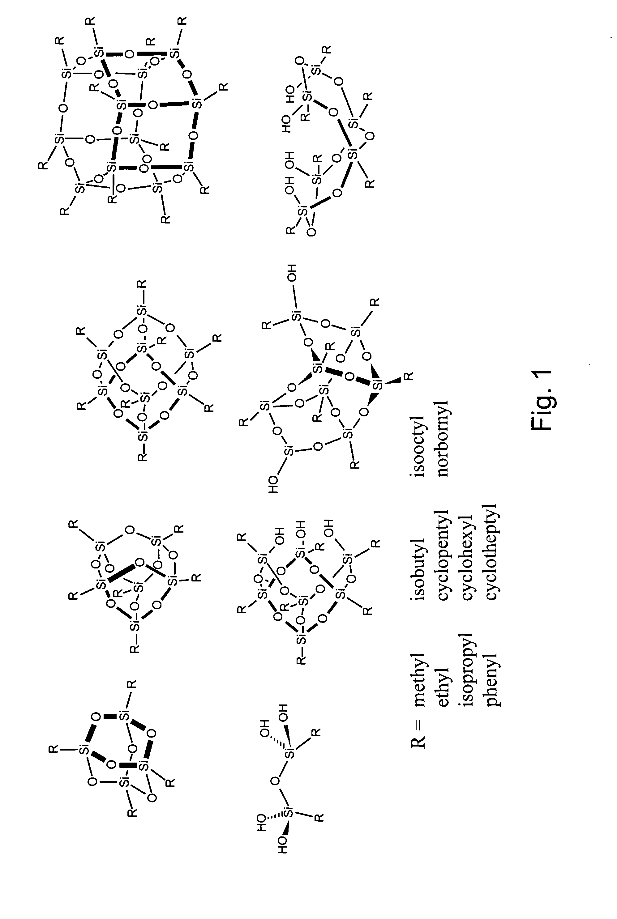
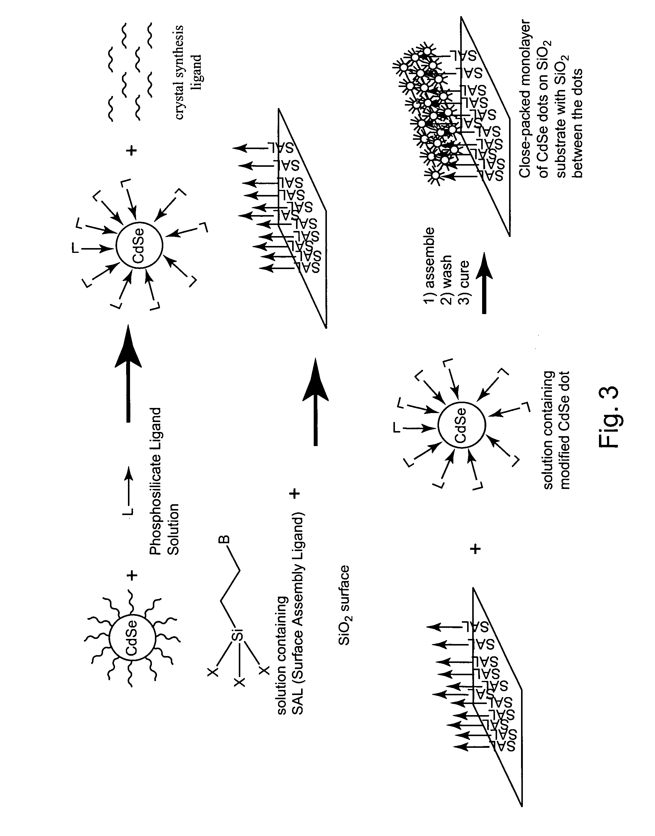
[0224]A method for preparing a substrate having closely packed nanostructures is depicted schematically in FIGS. 3 and 4. A nanodot (depicted as a sphere) is synthesized with surfactants that coat the surface. The surfactants are ligand-exchanged for the silsesquioxane or other silicate ligand (L).

[0225]A selected substrate (e.g., a silicon dioxide wafer) is coated with a silane ligand bearing a nanostructure binding head group (B). The silane ligands interact and associate into a self assembled monolayer of surface assembly ligand (SAL) on the substrate surface, providing a nanostructure-binding interface (as indicated by the perpendicular arrows). An exemplary surface assembly ligand includes a cyclic dimethyl amino moiety and a SiMe2 group coupled together via a linker (cyclic dimethyl amino-organic spacer-SiMe2).

[0226]The ligand exchanged nanodots are then put on the SAL substrate by spin coating or dip coating with the solve...

example 2

Synthesis of Heptacyclopentyl Poss Disilanol Diethoxyphosphate

[0227]Synthesis of the exemplary polyhedral oligomeric silsesquioxane (POSS) ligand heptacyclopentyl POSS disilanol diethoxyphosphate 2 was performed as provided herein (FIG. 6). All procedures were carried out under an inert atmosphere using Sclilenk technique. The solvents were dried over 4 Å molecular sieves and degassed with three freeze-vacuum-thaw cycles. The heptacyclopentyl POSS trisilanol 1 was dried by static vacuum in a dessicator with phosphorous pentoxide for 12 hours, and diethyl chlorophosphonate (Cl—P(O)(OEt)2 was vacuum transferred before use. Mass spectrometry was performed at Scripps Research Institute in La Jolla, and 31P {1H} NMR spectroscopy was performed with a Bruker FT NMR using 31P at 162 MHz.

[0228]The reaction was set up in a 50 mL Schlenk flask. Heptacyclopentyl POSS trisilanol 1 (1.00 g, 1.14 mmol) was dissolved in a combination of toluene (10 mL) and triethylamine (15 mL) and produced a clear...

example 3

Generation of a Monolayer of Coated Nanostructures on a SAM

[0236]The controlled self-assembly of monolayers of nanocrystals with silsesquioxane or silicate ligands tailored for charge storage applications can be achieved by various wet-process methods, such as the deposition onto self-assembled monolayers (SAMs). This approach can be used to prepare monolayers having close packed nanostructure arrays, and preferably ordered close-packed nanostructure arrays.

[0237]A self assembled monolayer consisting of a silane ligand with a binding head for the silsesquioxane or silicate ligand is applied to a substrate surface. The nanocrystals are deposited on the SAM from solution by spin-, dip-, or spray-coating, or conventional printing technologies. The excess dots are washed off the substrate resulting in a monolayer of nanocrystals insulated with silicon dioxide containing ligands.


PUM

PropertyMeasurementUnit
aspect ratioaaaaaaaaaa

Abstract

Ligand compositions for use in preparing discrete coated nanostructures are provided, as well as the coated nanostructures themselves and devices incorporating same. Methods for post-deposition shell formation on a nanostructure, for reversibly modifying nanostructures, and for manipulating the electronic properties of nanostructures are also provided. The ligands and coated nanostructures of the present invention are particularly useful for close packed nanostructure compositions, which can have improved quantum confinement and / or reduced cross-talk between nanostructures. Ligands of the present invention are also useful for manipulating the electronic properties of nanostructure compositions (e.g., by modulating energy levels, creating internal bias fields, reducing charge transfer or leakage, etc.).

Description

CROSS-REFERENCE TO RELATED APPLICATIONS[0001]This application claims priority to and benefit of U.S. Provisional Patent Application No. 60 / 635,799, filed Dec. 13, 2004, entitled “COMPOSITIONS AND METHODS FOR MODULATION OF NANOSTRUCTURE ENERGY LEVELS” by Jeffery A. Whiteford et al., and is a continuation-in-part of U.S. patent application Ser. No. 11 / 147,670, filed Jun. 7, 2005, now U.S. Pat. No. 7,267,875 entitled “POST-DEPOSITION ENCAPSULATION OF NANOSTRUCTURES: COMPOSITIONS, DEVICES AND SYSTEMS INCORPORATING SAME” by Jeffery A. Whiteford, et al., which claims priority to and benefit of the following prior provisional patent applications: U.S. Ser. No. 60 / 578,236, filed Jun. 8, 2004, entitled “POST-DEPOSITION ENCAPSULATION OF NANOCRYSTALS: COMPOSITIONS, DEVICES AND SYSTEMS INCORPORATING SAME” by Jeffery A. Whiteford et al., and U.S. Ser. No. 60 / 632,570, filed Nov. 30, 2004, entitled “POST-DEPOSITION ENCAPSULATION OF NANOSTRUCTURES: COMPOSITIONS, DEVICES AND SYSTEMS INCORPORATING SA...

Claims


Application Information

Patent Timeline
Patent Type & Authority Patents(United States)
IPC IPC(8): B32B5/16
CPCC07F5/025B05D5/12Y10T428/2993Y10T428/2991Y10T428/2995Y10T428/2998Y10T428/2996Y10T428/2982
Inventor WHITEFORD, JEFFERY A.BURETEA, MIHAI A.CHEN, JIANFREEMAN, WILLIAM P.MEISEL, ANDREASNGUYEN, LINHPARCE, J. WALLACESCHER, ERIK
Owner WODEN TECH INC
Learn More