Mask blank, transfer mask, method of manufacturing a transfer mask, and method of manufacturing a semiconductor device

a technology of transfer mask and mask blank, which is applied in the field of mask blank, transfer mask, and method of manufacturing transfer mask to achieve the effect of small bias

Active Publication Date: 2013-11-05
HOYA CORP
View PDF10 Cites 2 Cited by
  • Summary
  • Abstract
  • Description
  • Claims
  • Application Information

AI Technical Summary

Benefits of technology

[0011]Generally, in order to suppress the surface reflection of a light-shielding film, the surface reflectance of the light-shielding film is reduced by setting the degree of oxidation or nitridation of a material of a layer on the surface side (upper layer) to be higher than that of a material of a layer on the substrate side (lower layer). On the other hand, in a binary mask blank, a light-shielding film is required to have a predetermined or higher light-shielding performance (e.g. an optical density (OD) of 2.8 or more), while, as the degree of oxidation or nitridation of a material of the light-shielding film increases, the light-shielding performance of the light-shielding film decreases. In the meantime, due to the miniaturization of a transfer pattern in recent years, it has become necessary to use an oblique illumination method or an immersion exposure method. Further, following the miniaturization of the transfer pattern, the miniaturization and complication of an auxiliary pattern are remarkable. In order to cope with them, a reduction in the thickness of the light-shielding film has become necessary. Therefore, it is necessary to minimize the degree of oxidation or nitridation in the layer on the substrate side (lower layer) in order to ensure the light-shielding performance with as small a thickness as possible. On the other hand, the surface reflectance on the substrate side (back-surface reflectance) of the light-shielding film should also be suppressed to a predetermined value or less although not so low as the surface reflectance on the surface side (front-surface reflectance) of the light-shielding film, and thus, the lower layer of the light-shielding film should also be oxidized or nitrided to some extent.
[0014]According to the recent EB defect correction technique, using a passivation technique (supplying water, oxide-based gas, or the like) such as water passivation that lowers the etching rate by supplying water, it is possible to reduce the disadvantage even if there is some etching rate difference between the upper and lower layers of the light-shielding film. However, there is a limit to such etching rate control. Further, if the etching rate is excessively lowered, the correction time is prolonged so that the etching selectivity is reduced between the lower layer and a transparent substrate made of synthetic quartz or the like. As a consequence, there arise problems that a surface of the substrate is roughened, that etched recesses are locally formed on the substrate surface, and so on. Therefore, the laminated structure of the light-shielding film that requires the etching rate of the lower layer to be extremely lowered is not preferable.
[0018]This invention has been made in order to solve the conventional problems and has an object to provide a mask blank which enables a defect correction technique using charged particle irradiation to be suitably applied to a transfer mask manufactured from the mask blank and which can make small a bias for the transfer mask due to an electromagnetic field (EMF) effect, and further to provide such a transfer mask, a method of manufacturing such a transfer mask, and a method of manufacturing a semiconductor device using such a transfer mask.
[0021]First, the present inventors have paid attention to the fact that, in the case of a light-shielding film with a small influence of the EMF effect, it is easy to take advantage of the TMA simulation and thus to reduce the load of correction calculation for making an actual transfer pattern and a design transfer pattern coincide with each other. As a result of further studying a light-shielding film with a small influence of the EMF effect, it has been found that, by adjusting in predetermined ranges the contents of nitrogen in materials of a light-shielding film of a binary mask, it is possible not only to make small a bias due to the EMF effect, but also to solve the problems relating to the undercut which arise when the EB defect correction technique is applied to the conventional light-shielding film.
[0022]As a result of studying various materials, the present inventors have found that, in a mask blank comprising a light-shielding film having an at least two-layer structure comprising a lower layer composed of a material containing a transition metal, silicon, and nitrogen and an upper layer composed of a material containing a transition metal, silicon, and nitrogen, it is possible to solve the problems which arise when the EB defect correction technique is applied to the conventional light-shielding film, and further to make small a bias due to the EMF effect by adjusting the nitrogen content of the material of the lower layer to 21 at % or more and the refractive index n of the lower layer to 1.9 or less, adjusting the refractive index n of the upper layer to 2.1 or less, and adjusting the nitrogen content of a surface layer, in which oxygen is inevitably contained, of the upper layer to 14 at % or more, and have completed this invention.
[0089]According to this invention, it is possible to provide a mask blank which enables a defect correction technique using charged particle irradiation to be suitably applied to a transfer mask manufactured from the mask blank and which can make small a bias for the transfer mask due to an electromagnetic field (EMF) effect, and further to provide such a transfer mask, a method of manufacturing such a transfer mask, and a method of manufacturing a semiconductor device using such a transfer mask.

Problems solved by technology

As a result, it has been found that the following problems may occur depending on the relationship between the film compositions in the upper and lower layers of the laminated structure.
However, in the case of nitrided, oxidized, or carbonized silicon such as Si3N4, SiO2, SiON, or SiC, a highly volatile high-order fluoride is not easily formed so that there is a tendency of having high etching resistance to a fluorine-based gas such as a XeF2 gas.

Method used


Image

  • Mask blank, transfer mask, method of manufacturing a transfer mask, and method of manufacturing a semiconductor device
  • Mask blank, transfer mask, method of manufacturing a transfer mask, and method of manufacturing a semiconductor device
  • Mask blank, transfer mask, method of manufacturing a transfer mask, and method of manufacturing a semiconductor device

Examples


example 1

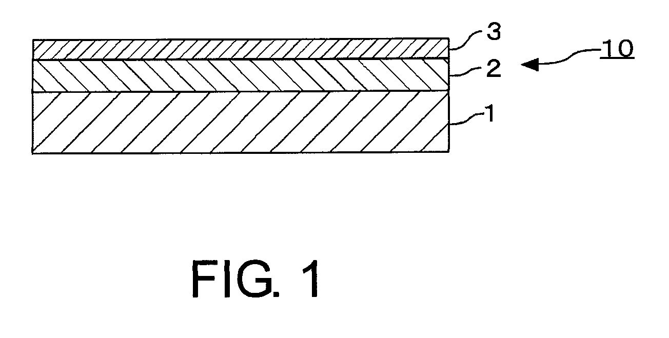
[0135]In a single-wafer sputtering apparatus, using a mixed target of molybdenum (Mo) and silicon (Si) (at % ratio Mo:Si=13:87) as a sputtering target, reactive sputtering (DC sputtering) was carried out in a mixed gas atmosphere of argon and nitrogen, thereby forming a MoSiN film (lower layer (light-shielding layer)) to a thickness of 47 nm on a transparent substrate 1 made of synthetic quartz glass. Then, using a Mo / Si target (at % ratio Mo:Si=13:87), reactive sputtering (DC sputtering) was carried out in a mixed gas atmosphere of argon and nitrogen, thereby forming a MoSiN film (upper layer (front-surface antireflection layer)) to a thickness of 4 nm on the lower MoSiN film. In this manner, a light-shielding film 2 (total thickness: 51 nm) for ArF excimer laser light (wavelength: 193 nm) was formed.

[0136]Then, the substrate 1 with the light-shielding film 2 was heat-treated (annealed) at 450° C. for 30 minutes, thereby reducing the film stress of the light-shielding film 2. A sub...

example 2

[0137]In a single-wafer sputtering apparatus, using a mixed target of molybdenum (Mo) and silicon (Si) (at % ratio Mo:Si=13:87) as a sputtering target, reactive sputtering (DC sputtering) was carried out in a mixed gas atmosphere of argon and nitrogen, thereby forming a MoSiN film (lower layer (light-shielding layer)) to a thickness of 46 nm on a transparent substrate 1 made of synthetic quartz glass. Then, using a Mo / Si target (at % ratio Mo:Si=13:87), reactive sputtering (DC sputtering) was carried out in a mixed gas atmosphere of argon and nitrogen, thereby forming a MoSiN film (upper layer (front-surface antireflection layer)) to a thickness of 3 nm on the lower MoSiN film. In this manner, a light-shielding film 2 (total thickness: 49 nm) for ArF excimer laser light (wavelength: 193 nm) was formed.

[0138]Then, the substrate 1 with the light-shielding film 2 was heat-treated (annealed) at 450° C. for 30 minutes, thereby reducing the film stress of the light-shielding film 2. A sub...

reference example 1

[0139]In a single-wafer sputtering apparatus, using a mixed target of molybdenum (Mo) and silicon (Si) (at % ratio Mo:Si=13:87) as a sputtering target, reactive sputtering (DC sputtering) was carried out in a mixed gas atmosphere of argon and nitrogen, thereby forming a MoSiN film (lower layer (light-shielding layer)) to a thickness of 47 nm on a transparent substrate 1 made of synthetic quartz glass. Then, using a Mo / Si target (at % ratio Mo:Si=13:87), reactive sputtering (DC sputtering) was carried out in a mixed gas atmosphere of argon and nitrogen, thereby forming a MoSiN film (upper layer (front-surface antireflection layer)) to a thickness of 13 nm on the lower MoSiN film. In this manner, a light-shielding film 2 (total thickness: 60 nm) for ArF excimer laser light (wavelength: 193 nm) was formed.

[0140]Then, the substrate 1 with the light-shielding film 2 was heat-treated (annealed) at 450° C. for 30 minutes, thereby reducing the film stress of the light-shielding film 2. A su...


PUM

PropertyMeasurementUnit
refractive indexaaaaaaaaaa
thicknessaaaaaaaaaa

Abstract

A mask blank for use in the manufacture of a transfer mask adapted to be applied with ArF excimer laser exposure light is disclosed. The mask blank has, on a transparent substrate, a light-shielding film for forming a transfer pattern. The light-shielding film has an at least two-layer structure including a lower layer and an upper layer from the transparent substrate side. The lower layer is made of a material composed of a transition metal, silicon, and nitrogen and having a nitrogen content of 21 at % or more and a refractive index n of 1.9 or less. The upper layer is made of a material composed of a transition metal, silicon, and nitrogen and having a refractive index n of 2.1 or less. A surface layer of the upper layer contains oxygen and has a nitrogen content of 14 at % or more.

Description

[0001]This application is based upon and claims the benefit of priority from Japanese Patent Application No. 2010-281333, filed on Dec. 17, 2010, the disclosure of which is incorporated herein in its entirety by reference.TECHNICAL FIELD[0002]This invention relates to a mask blank, a transfer mask, a method of manufacturing a transfer mask, and a method of manufacturing a semiconductor device. In particular, this invention relates to a mask blank which enables a defect correction technique using charged particle irradiation to be suitably applied to a transfer mask manufactured from the mask blank and which can make small a bias for the transfer mask due to an electromagnetic field (EMF) effect, and further relates to such a transfer mask, a method of manufacturing such a transfer mask, and a method of manufacturing a semiconductor device using such a transfer mask.BACKGROUND ART[0003]Generally, fine pattern formation is carried out by the photolithography in the manufacture of a se...

Claims


Application Information

Patent Timeline
Patent Type & Authority Patents(United States)
IPC IPC(8): G03F1/50
CPCG03F1/58G03F1/00G03F1/74G03F7/2006G03F1/50Y10T428/24942G03F1/38G03F1/46H01L21/0274H01L21/0337
Inventor KOMINATO, ATSUSHIHASHIMOTO, MASAHIROIWASHITA, HIROYUKI
Owner HOYA CORP
Why Eureka
Try Eureka