Method for forming group III/V conformal layers on silicon substrates

a technology of conformal layers and silicon substrates, applied in the direction of crystal growth process, polycrystalline material growth, chemically reactive gases, etc., can solve the problems of generating defects, iii/v materials on silicon substrates, and many challenges

Active Publication Date: 2013-12-10
APPLIED MATERIALS INC
View PDF23 Cites 23 Cited by
  • Summary
  • Abstract
  • Description
  • Claims
  • Application Information

AI Technical Summary

Benefits of technology

[0060]Thus, methods for the deposition of a conformal group III / V layer over a silicon substrate having a group III nucleation layer are provided. The novel method of epitaxially growing a group III / V layer has numerous advantages over the prior art including formation on any surface orientation, much thinner layers, faster throughput and higher quality crystalline structures. This is beneficial for the production of any feature that requires the deposition of group III / V layers, such as CMOS production. Exposed regions of silicon can be covered by the conformal group III layer which allows for the deposition of conformal subsequent group III / V layers.
[0061]While the foregoing is directed to embodiments of the present invention, other and further embodiments of the invention may be devised without departing from the basic scope thereof, and the scope thereof is determined by the claims that follow.

Problems solved by technology

Despite the advantages and utility of such layers, the growth of group III / V materials on silicon substrates presents many challenges.
When the lattice mismatch between the epitaxial layer and substrate exceeds a few percent, the strain induced by the mismatch becomes too great and defects are generated in the epitaxial layer when the epitaxial film relaxes.
Many defects, particularly threading dislocations, tend to propagate into the “device layer” where the semiconductor device is fabricated.
However, layer uniformity between different surface orientations of the silicon substrate has remained a constant problem.
A related difficulty to depositing group III / V layers for CMOS features is conformal deposition on silicon substrates.
As such, the formation of a conformal layer on different crystal orientations requires the deposition of a thick layer to accommodate for above crystal defects which is not optimal for small feature formation in CMOS.

Method used


Image

  • Method for forming group III/V conformal layers on silicon substrates
  • Method for forming group III/V conformal layers on silicon substrates
  • Method for forming group III/V conformal layers on silicon substrates

Examples


Embodiment Construction

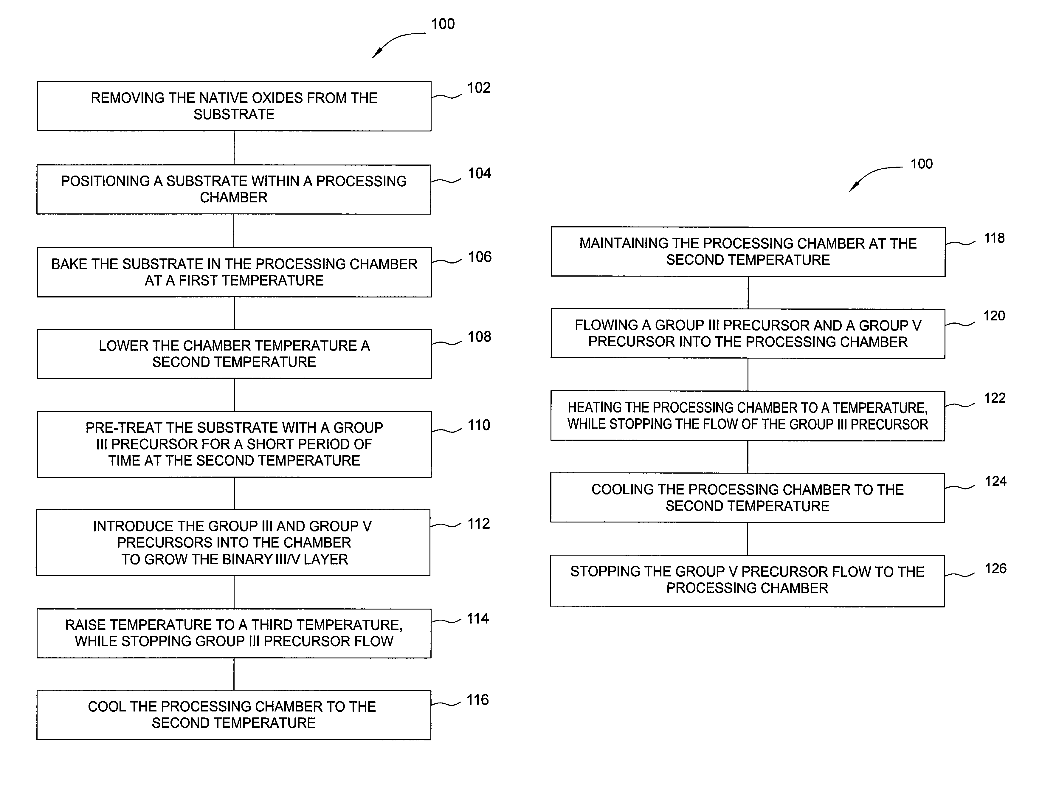
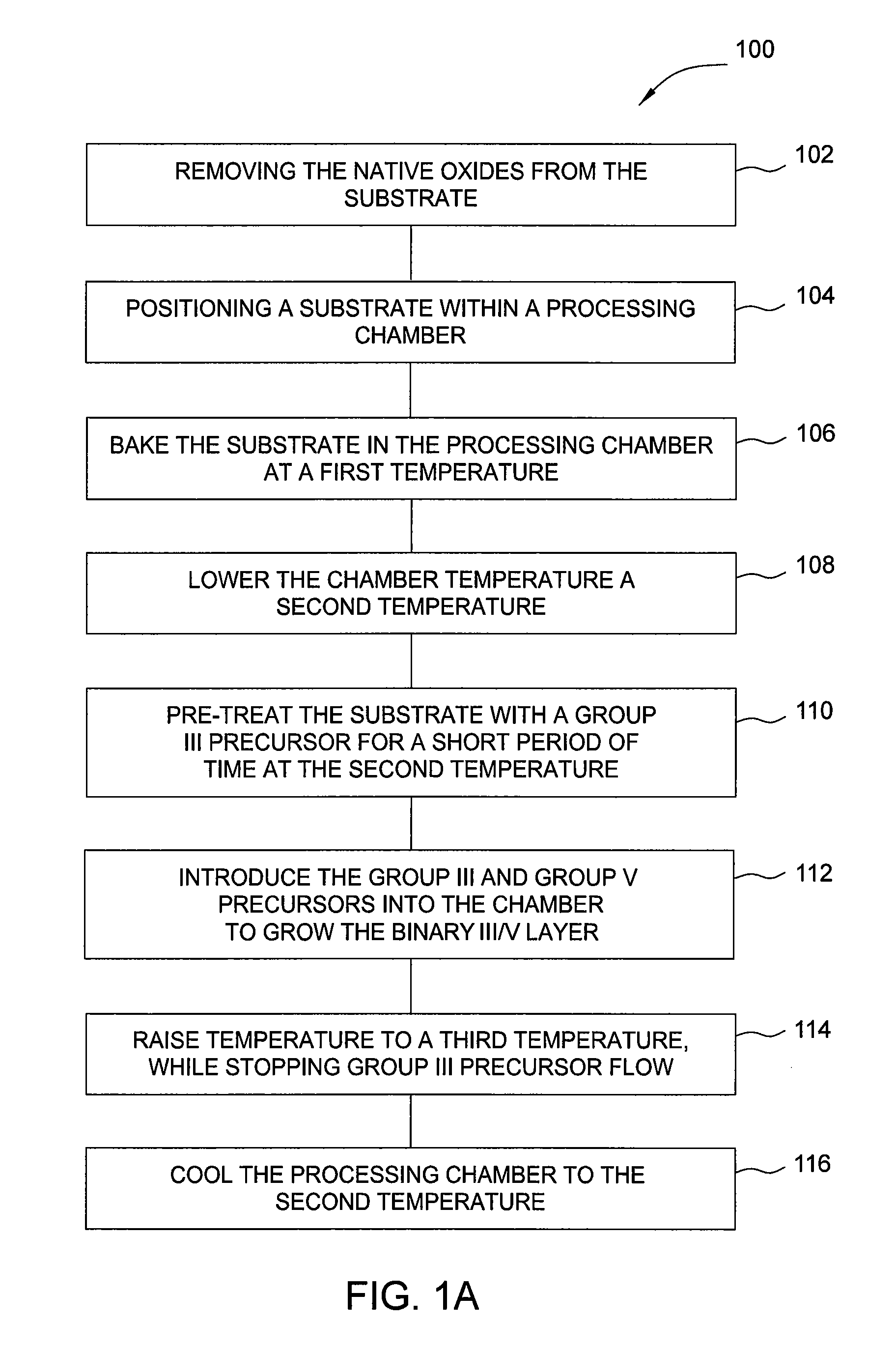
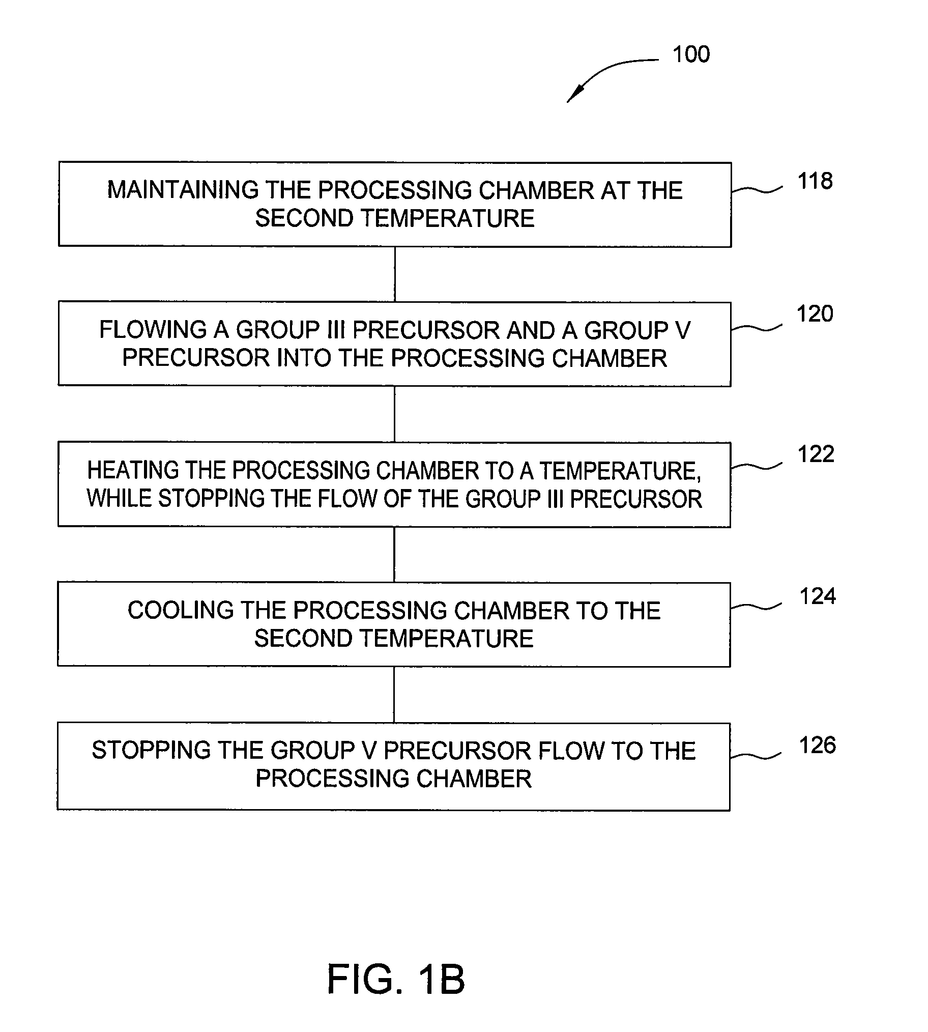
[0023]Embodiments of the invention generally relate to methods for forming group III / V materials on silicon surfaces and the resulting composition forming a buffer layer on a nucleation layer composed of a group III element. In one embodiment, a method for forming a conformal layer on a substrate is provided which can include removing the native oxide from the substrate, positioning a substrate within a processing chamber, heating the substrate to a first temperature, cooling the substrate to a second temperature, and flowing a group III precursor into the processing chamber. The group III precursor can be selected from all known group III precursors.

[0024]The first temperature, which can correspond to a post cleaning step, can range from about 400° C. to about 800° C., with preferred embodiments ranging from about 400° C. to about 500° C. The post cleaning step can be used to remove remaining contaminants from the surface of the substrate. The second temperature, which can correspo...


PUM

PropertyMeasurementUnit
temperatureaaaaaaaaaa

Abstract

A method for forming a conformal group III / V layer on a silicon substrate and the resulting substrate with the group III / V layers formed thereon. The method includes removing the native oxide from the substrate, positioning a substrate within a processing chamber, heating the substrate to a first temperature, cooling the substrate to a second temperature, flowing a group III precursor into the processing chamber, maintaining the second temperature while flowing a group III precursor and a group V precursor into the processing chamber until a conformal layer is formed, heating the processing chamber to an annealing temperature, while stopping the flow of the group III precursor, and cooling the processing chamber to the second temperature. Deposition of the III / V layer may be made selective through the use of halide gas etching which preferentially etches dielectric regions.

Description

BACKGROUND OF THE INVENTION[0001]1. Field of the Invention[0002]Embodiments of the invention generally relate to processes for forming group III / V materials on a silicon substrate using a group III nucleation layer.[0003]2. Description of the Related Art[0004]Group III / V semiconductors have significant potential as useful materials in high-temperature, high frequency and high power microelectronics and ultra-violet / blue / green optoelectronics by virtue of their wide bandgaps, high thermal conductivities and large electrical breakdown fields. Microelectronic device applications include AlGaNGaN multilayer-based laser diodes, high electron mobility transistors (HEMTs), field effect transistors (FETs), heterojunction bipolar transistors (HBTs), light emitting diodes (LEDs) and ultra-violet photodetectors, as well as (Al,In,Ga) N-based devices generally, including devices for high-frequency, high-power communications, for high-density optical storage, full-color displays, and for other w...

Claims


Application Information

Patent Timeline
Patent Type & Authority Patents(United States)
IPC IPC(8): H01L21/20C30B11/00C30B28/14C30B28/12C30B25/00C30B23/00C30B35/00H01L21/36
CPCH01L21/02381H01L21/02455H01L21/0262H01L29/267H01L21/02538Y10T117/1008H01L21/324H01L29/78H01L29/778H01L21/02694H01L29/205
Inventor BAO, XINYUSANCHEZ, ERROL ANTONIO C.CARLSON, DAVID K.YE, ZHIYUAN
Owner APPLIED MATERIALS INC
Why Eureka
Try Eureka