Differential delay cell with low power, low jitter, and small area

a differential delay and cell technology, applied in the field of delay cells, can solve the problems of increasing the noise environment in which plls and dlls must function, reducing the stability around the operating frequency, and the design of low jitter plls and dlls has become very difficult, so as to improve the deterministic noise performance, reduce the amount of noise supplied, and reduce the power supply voltage

Inactive Publication Date: 2013-12-17
MONTEREY RES LLC
View PDF22 Cites 3 Cited by
  • Summary
  • Abstract
  • Description
  • Claims
  • Application Information

AI Technical Summary

Benefits of technology

[0016]As noted above, at least one swing limiting transistor may be coupled between the drain terminals of the current source transistors. In one embodiment, a single swing limiting transistor may be coupled between the drain terminals of the current source transistors. In another embodiment, the single swing limiting device may be replaced with two back to back diode-connected swing limiting devices. The swing limiting transistor(s) may be included, for example, to control the output swing of the delay cell and to keep the current source transistors in saturation.
[0017]In some cases, an RC filter may be coupled to the delay cell architecture to reduce the amount of noise supplied thereto. For example, the RC filter may be connected between the power supply bus and the mutually-coupled source terminals of the current source transistors for supplying a reduced power supply voltage thereto. In some cases, the RC filter may also be connected to the gate terminal of the single swing limiting transistor.
[0018]The RC filter may be implemented in a variety of ways. In some cases, the RC filter may include a resistor and a capacitor. To improve deterministic noise performance, the RC filter may include a relatively large resistor and relatively small capacitor. As known in the art, increasing the RC product reduces the cut-off frequency of the low pass RC filter. For a given C, a larger R may be used to reduce the cut-off frequency and improve noise rejection. In some cases, a relatively large resistor may be used to reduce the amount of area consumed by the delay cell (e.g., up to about 58% less area), while providing up to 90% less deterministic jitter in the generated output signals. Reduced current consumption (e.g., up to about 23% less current) and phase-induced jitter (e.g., up to 7% less phase jitter) may also be provided by removing an additional current source, which is typically coupled between the RC filter and the first and second current source transistors.

Problems solved by technology

Unfortunately, the rising demand for high-speed electronics has created an increasingly noisy environment in which PLLs and DLLs must function.
Jitter is undesirable because it often leads to decreased stability around the operating frequency (or “center frequency”) of the PLL / DLL device.
With a shrinking tolerance for jitter in the decreasing period of the output clock, the design of low jitter PLLs and DLLs has become very challenging.
Unfortunately, the loop bandwidth is affected by many process technology factors, and as a result, is often constrained well below the lowest operating frequency needed for stability.
Although VCOs have recently been fabricated using CMOS technology to obtain higher operating frequencies (e.g., several Gigahertz, GHz) and to meet the increasing demand for lower cost and higher integration, phase-noise reduction remains a challenge for typical CMOS voltage controlled oscillators.
Although CMOS LC-tank oscillators provide some improvement in phase noise performance, they have not been able overcome several barriers preventing them from becoming a reliable VCO.
One such barrier is that the implementation of a high-quality inductor in a standard CMOS process is limited by parasitic effects and usually requires extra non-standard processing steps.
Another barrier is that the LC-tank oscillator often demonstrates a narrow tuning range, causing PLL performance to be sensitive to process variations.
However, the ring oscillator is not without limitations and usually demonstrates worse phase noise performance than the LC-tank oscillator.
However, conventional delay cells consume large amounts of current and area, and often fail to reduce phase noise components to acceptable levels.

Method used


Image

  • Differential delay cell with low power, low jitter, and small area
  • Differential delay cell with low power, low jitter, and small area
  • Differential delay cell with low power, low jitter, and small area

Examples


Embodiment Construction

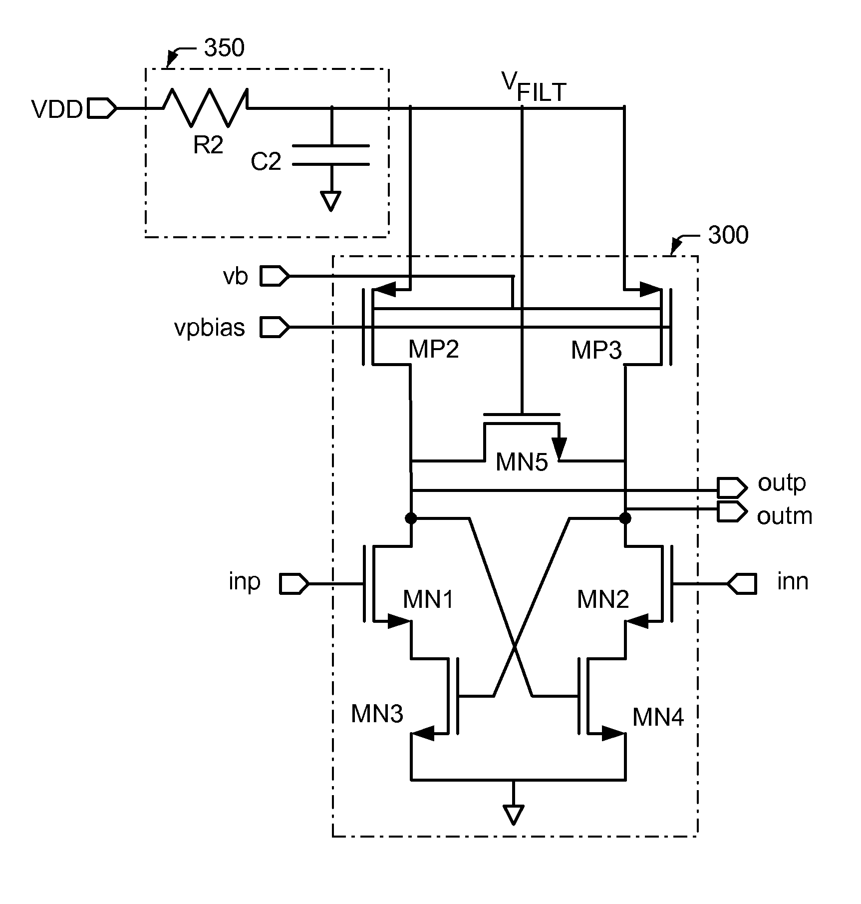
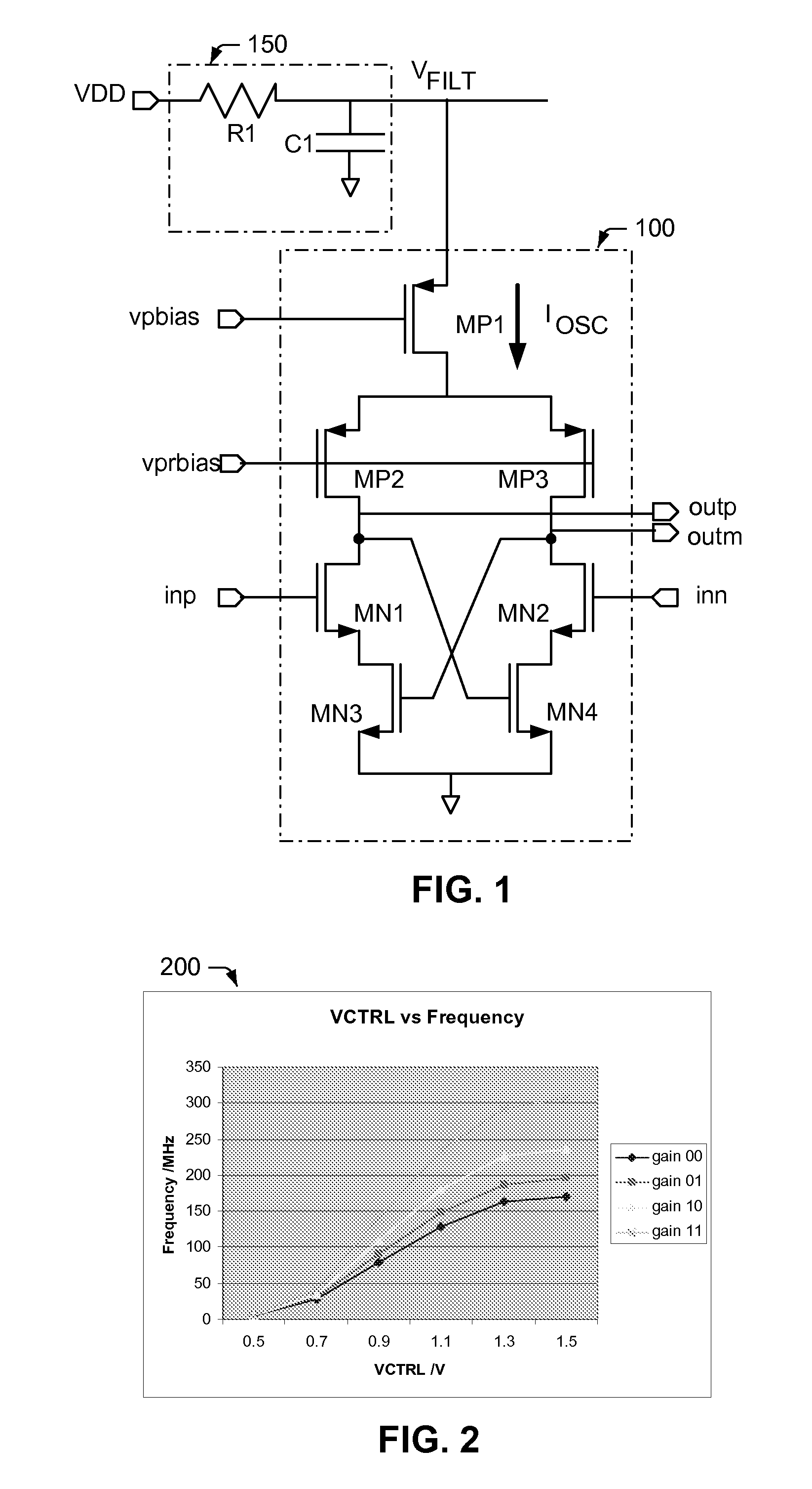
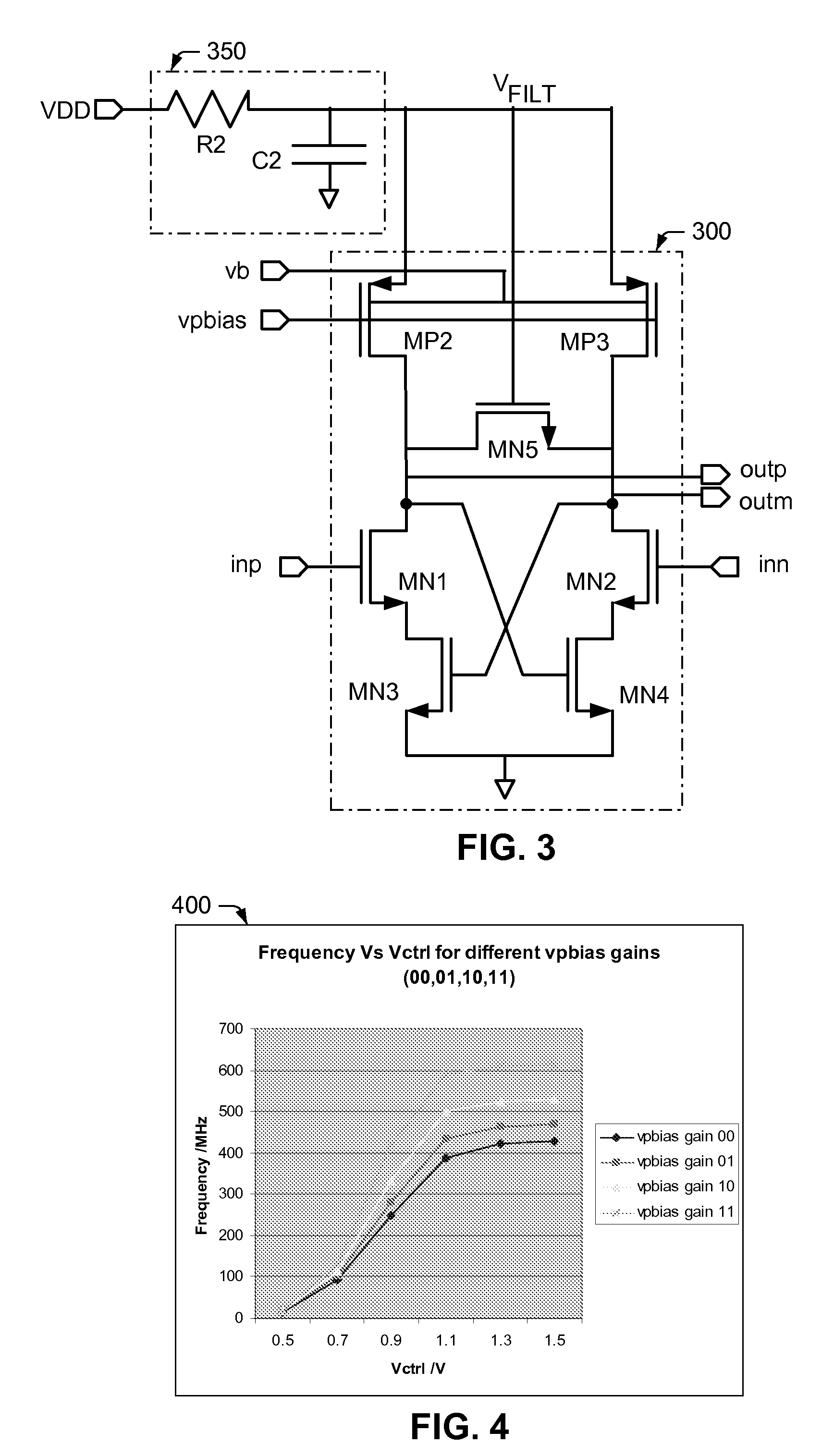
[0038]One embodiment of a low power differential delay cell 100 with programmable gain, frequency range and output swing is shown in FIG. 1. As illustrated, delay cell 100 includes a pair of input transistors (MN1, MN2), a pair of cross-coupled transistors (MN3, MN4), a pair of swing limiting transistors (MP2 and MP3) and a current source transistor (MP1). In some embodiments, delay cell 100 may be implemented with metal oxide semiconductor (MOS) transistors, as shown in FIG. 1. For example, the input and cross-coupled transistors may be implemented with NMOS transistors, while the current source and swing limiting transistors are implemented with PMOS transistors. However, delay cell 100 is not limited to MOS technology and may be alternatively implemented with other process technologies (e.g., bipolar).

[0039]During operation, a pair of differential input signals (inn, inp) is supplied to the gate terminals of the input transistors (MN1 and MN2). The potential difference between th...


PUM


Abstract

A delay cell architecture is provided herein with improved noise performance and increased output swing, while consuming less power and area than conventional delay cell architectures. In one embodiment, the delay cell described herein may include a pair of input transistors, a pair of cross-coupled transistors, a pair of current source transistors, at least one swing limiting transistor and an RC filter. The at least one swing limiting transistor is coupled between the output nodes of the delay cell for controlling the output swing and keeping the current source transistors in saturation. Phase-induced jitter is reduced by connecting the RC filter directly to the mutually-coupled source terminals of the current source transistors. Deterministic jitter is reduced by using a relatively large resistor and relatively small capacitor within the RC filter design. Such a design reduces the amount of area consumed by the delay cell without sacrificing noise performance. Current consumption is reduced by requiring only one bias voltage to be supplied to the delay cell.

Description

PRIORITY CLAIM[0001]The present application claims priority to U.S. Provisional Application No. 60 / 826,120 filed Sep. 19, 2006.BACKGROUND OF THE INVENTION[0002]1. Field of the Invention[0003]This invention relates to delay cells and, more particularly, to differential delay cells with reduced power, jitter and area. The differential delay cells may be incorporated, e.g., within a voltage controlled oscillator (VCO) of a phase locked loop (PLL) or a delay line of a delay locked loop (DLL).[0004]2. Description of the Related Art[0005]The following descriptions and examples are given as background only.[0006]Phase-locked loops (PLLs) and delay-locked loops (DLLs) are routinely used for data and telecommunications, frequency synthesis, clock recovery, and similar applications. In some cases, for example, PLLs and DLLs may be used in the I / O interfaces of digital integrated circuits to hide clock distribution delays and to improve overall system timing. In general, a PLL or DLL may be us...

Claims


Application Information

Patent Timeline
Patent Type & Authority Patents(United States)
IPC IPC(8): H03H11/26H03K5/135
CPCH03K5/135
Inventor WALSH, PAUL M.
Owner MONTEREY RES LLC
Why Eureka
Try Eureka