Methods for directed self-assembly process/proximity correction

Active Publication Date: 2014-03-04
GLOBALFOUNDRIES US INC
View PDF15 Cites 22 Cited by
  • Summary
  • Abstract
  • Description
  • Claims
  • Application Information

AI Technical Summary

Benefits of technology

[0014]This brief summary is provided to introduce a selection of concepts in a simplified form that are further described below in the detailed description. This summary is not in

Problems solved by technology

However, the dimensions of features formed using conventional optical lithography techniques for volume manufacturing (e.g., 193 nm dry and immersion lithography) have reached the resolution limit of the lithographic tools.
The creation of vias with smaller critical dimensions (CDs), tighter pitches, and better CD uniformity is one of major challenges for future technology nodes; however, printing such via patterns beyond the 22 nm node is expected to be difficult using conventional optical lithography, even with expensive and complicated double patterning processes, resolution enhancement technology (computational lithography) and severe layout design restrictions.
Unfortunately, no alternative non-optical lithographic technique with higher resolution capabilities, such as e-beam lithography or extreme ultraviolet lithography (EUV), appears to be ready for high volume manufacturing in the near future.
While e-beam direct write lithography is capable of very high resolution, it is a direct-write technique and cannot achieve the necessary wafer throughput levels to make it viable for volume manufacturing.
EUV lithography tools have been under development for many years; however, many challenges associated with the source, collection optics, masks, and resists still remain and will lik

Method used


Image

  • Methods for directed self-assembly process/proximity correction
  • Methods for directed self-assembly process/proximity correction
  • Methods for directed self-assembly process/proximity correction

Examples


Embodiment Construction

[0017]The following detailed description is merely exemplary in nature and is not intended to limit the invention or the application and uses of the invention. As used herein, the word “exemplary” means “serving as an example, instance, or illustration.” Thus, any embodiment described herein as “exemplary” is not necessarily to be construed as preferred or advantageous over other embodiments. All of the embodiments described herein are exemplary embodiments provided to enable persons skilled in the art to make or use the invention and not to limit the scope of the invention which is defined by the claims. Furthermore, there is no intention to be bound by any expressed or implied theory presented in the preceding technical field, background, brief summary, or the following detailed description.

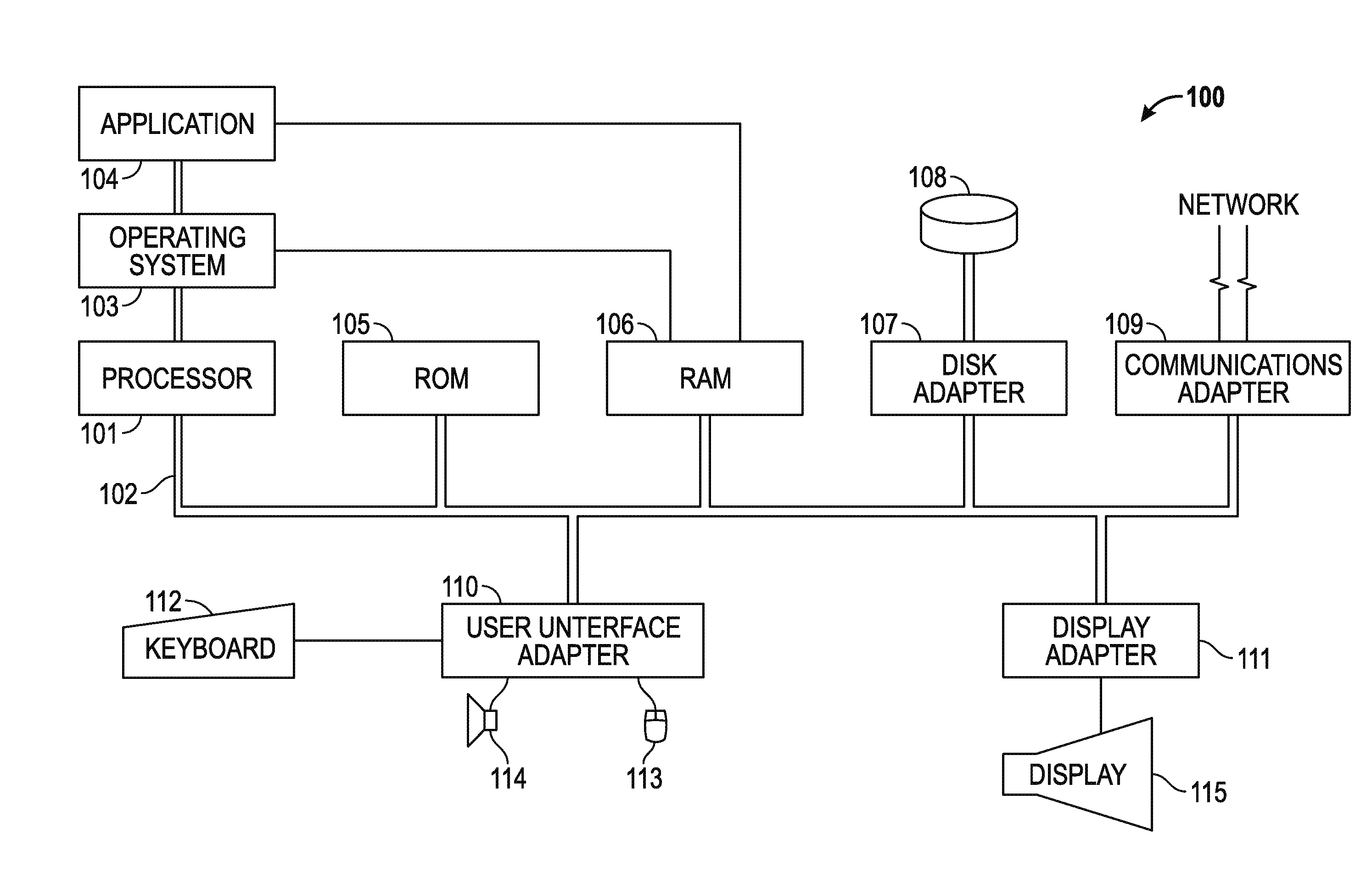
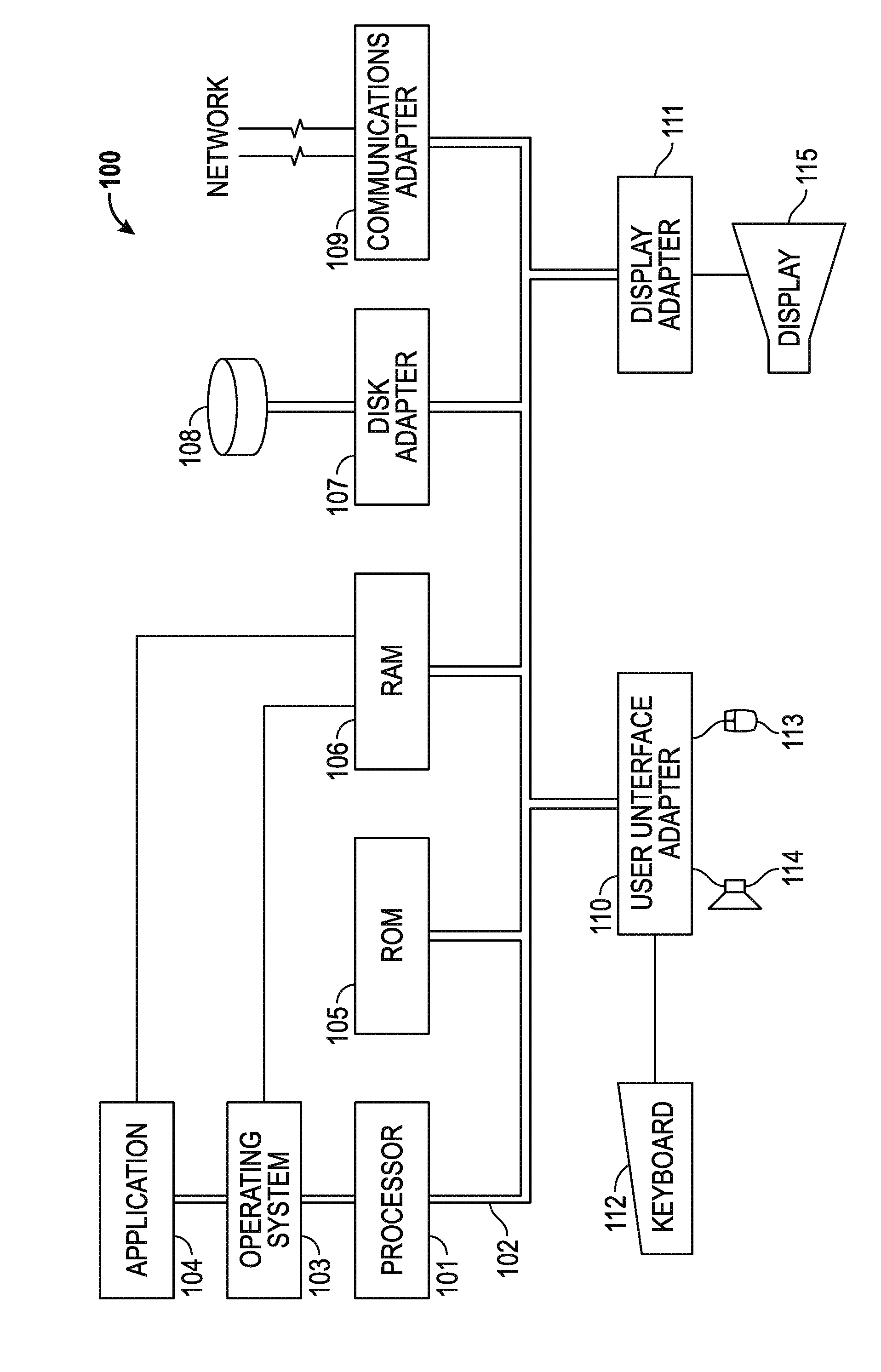
[0018]The present invention is a method of designing an optical photomask for forming a pre-pattern opening in a photoresist layer on a substrate wherein the photoresist layer and the prepatter...


PUM


Abstract

A method of fabricating an integrated circuit includes designing an optical photomask for forming a pre-pattern opening in a photoresist layer on a semiconductor substrate, wherein the photoresist layer and the pre-pattern opening are coated with a self-assembly material that undergoes directed self-assembly (DSA) to form a DSA pattern. Designing the optical photomask includes using a computing system, inputting a DSA target pattern, and using the computing system, applying a DSA model to the DSA target pattern to generate a first DSA directing pattern. Further, the step of designing the optical photomask includes using the computing system, calculating a residual between the DSA target pattern and the DSA directing pattern, and using the computing system, applying the DSA model to the first DSA directing pattern and the residual to generate a second, updated DSA directing pattern. Generating the second, updated DSA directing pattern includes linearizing a self-consistent field theory equation.

Description

CROSS-REFERENCE TO RELATED APPLICATIONS[0001]This application is a continuation-in-part of U.S. patent application Ser. No. 13 / 659,453, filed 24 Oct. 2012, and titled: “METHODS FOR DIRECTED SELF-ASSEMBLY PROCESS / PROXIMITY CORRECTION,” the contents of which are herein incorporated by reference in their entirety.TECHNICAL FIELD[0002]Embodiments of the present disclosure are directed to methods for manufacturing integrated circuits. More particularly, embodiments of the present disclosure are directed to methods for directed self-assembly process / proximity correction (DSA PC) in the design of integrated circuits (IC).BACKGROUND[0003]A semiconductor device typically includes a network of circuits that are formed over a substrate. The device may consist of several layers of circuit wiring, with various interconnects being used to connect these layers to each other and any underlying transistors. Generally, as a part of the manufacturing process, vias or contact holes are formed, which ar...

Claims


Application Information

Patent Timeline
IPC IPC(8): G06F17/13G06F17/11G06F17/50G03F1/00G21K5/00G06F19/00
CPCG06F19/00G06F17/5081G06F17/11G06F2217/12G06F17/13G03F1/70G03F1/36G06F17/5068G03F7/0002G06F30/398G06F2119/18Y02P90/02G16Z99/00
Inventor LATYPOV, AZAT
Owner GLOBALFOUNDRIES US INC
Why Eureka
Try Eureka