Method of producing a photonic device and corresponding photonic device

a photonic device and photonic technology, applied in the field of silicon photonics, can solve the problems of inability to optimize the performance of lasers and photodetectors independently, in terms of layer thickness and composition, and inability to use techniques for some important and common applications, and achieve the effect of simplifying the process

Inactive Publication Date: 2014-03-18
INTERUNIVERSITAIR MICRO ELECTRONICS CENT (IMEC VZW) +3
View PDF5 Cites 5 Cited by
  • Summary
  • Abstract
  • Description
  • Claims
  • Application Information

AI Technical Summary

Benefits of technology

[0026]This embodiment makes simpler the process according to the invention.

Problems solved by technology

However, silicon has a very poor photon emission efficiency.
However, the drawback of this configuration is that the lasers and photodetectors performances cannot be optimized independently, in terms of layer thickness and composition.
However, the major drawback of this technique is that the distance between a source and a photodetector is ruled by the size of the dice (usually 5 mm×5 mm) and the minimum distance allowed to bond dice (usually several millimetres).
Therefore, this technique cannot be used for some important and common applications where, for instance, a monitoring photodiode has to be implemented in close proximity of a laser, that is to say, at a distance of tens of μm.

Method used


Image

  • Method of producing a photonic device and corresponding photonic device
  • Method of producing a photonic device and corresponding photonic device
  • Method of producing a photonic device and corresponding photonic device

Examples


Embodiment Construction

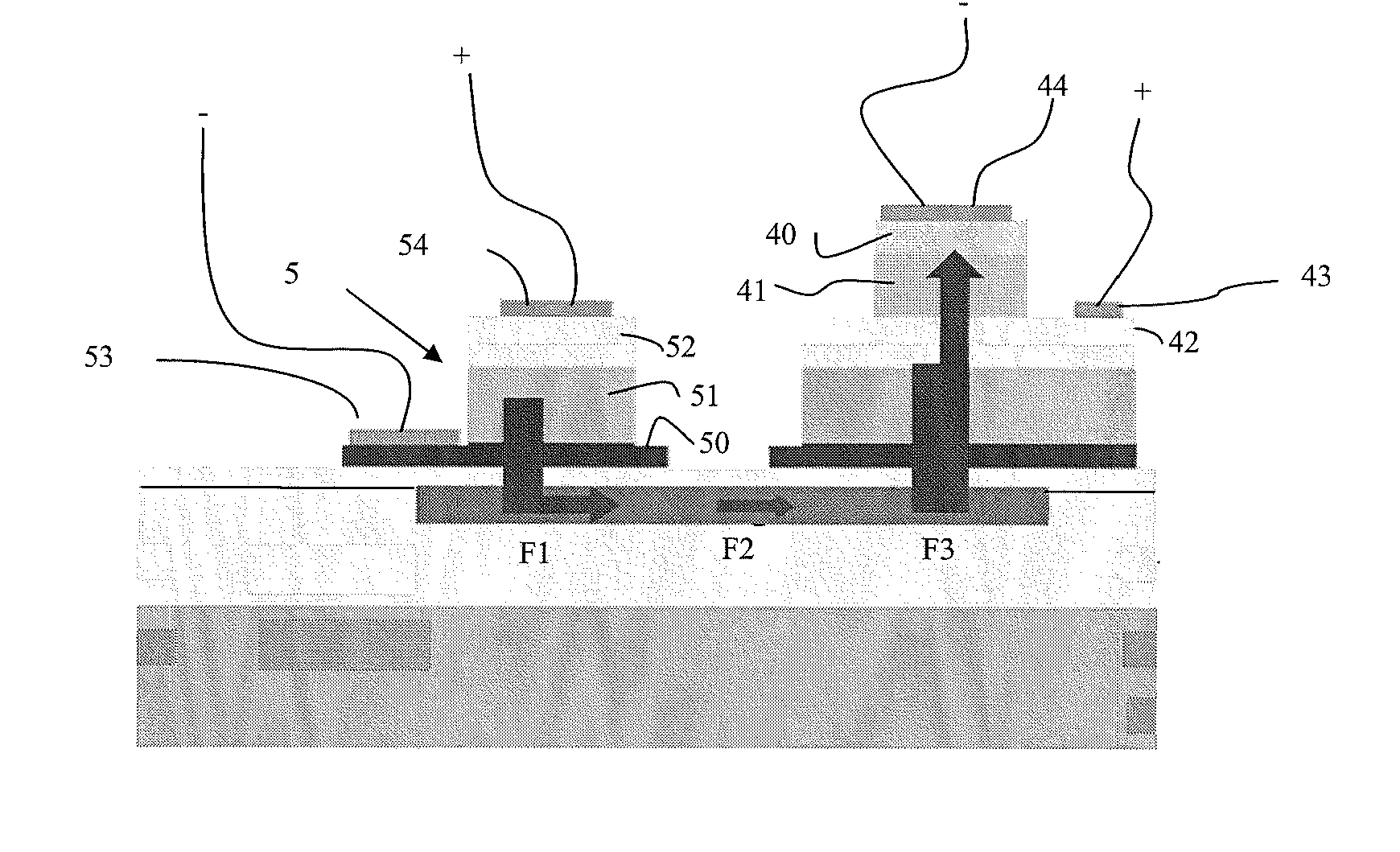
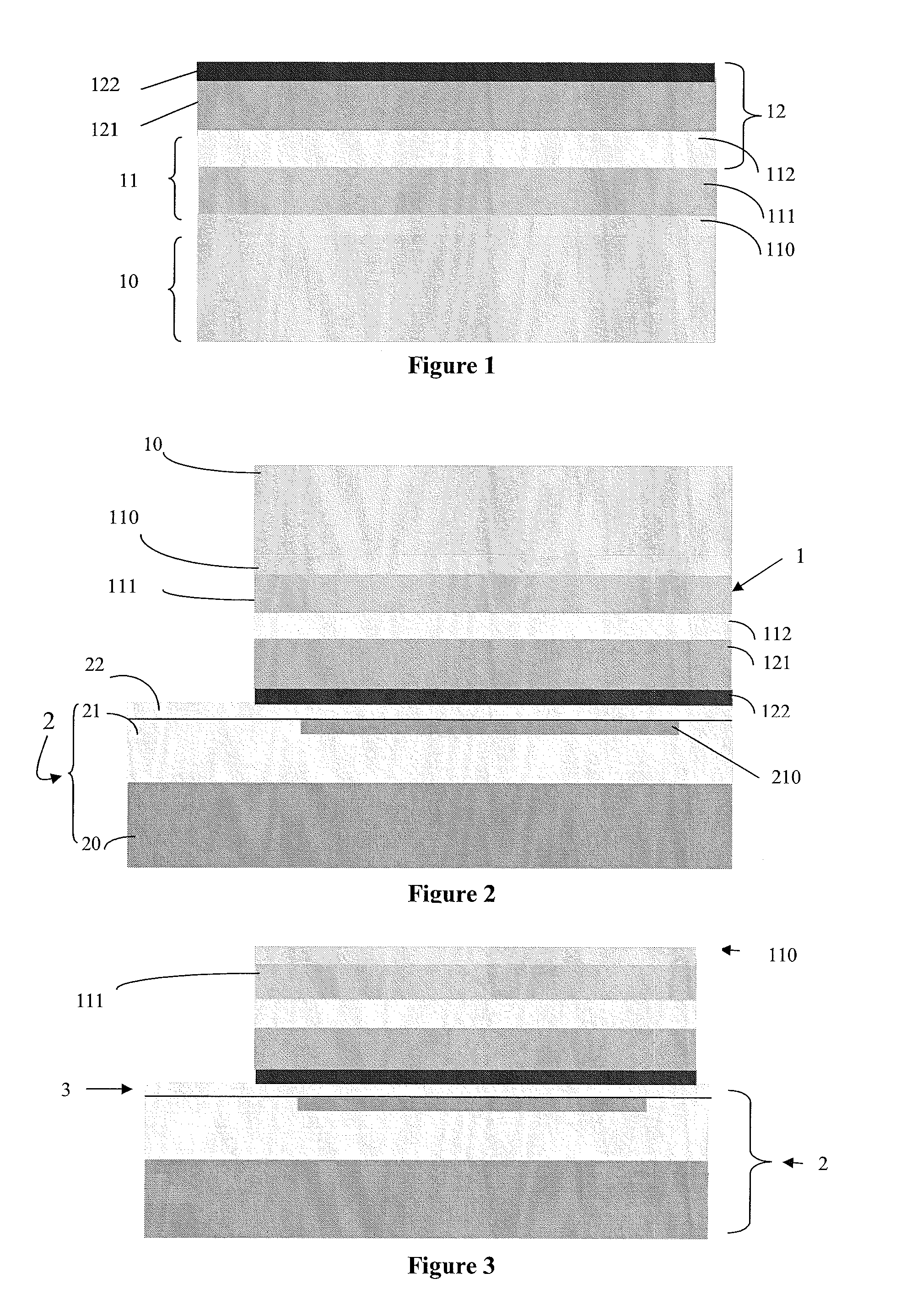
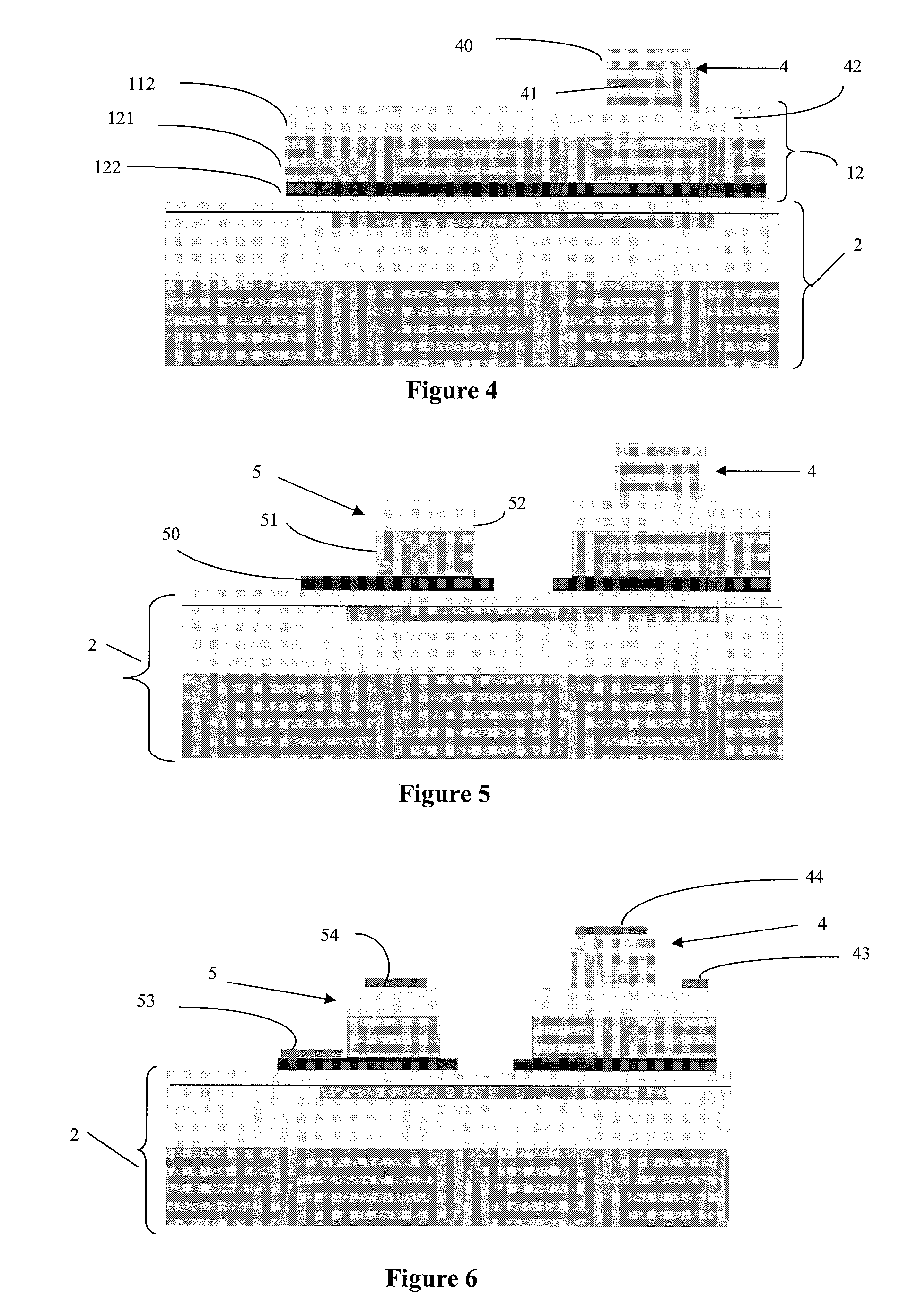
[0039]FIG. 1 illustrates the first step of the method according to the invention by showing an epitaxial structure 1 obtained by any suitable process, typically by means of metal organic chemical vapour deposition MOCVD or molecular beam epitaxy MBE techniques.

[0040]The process is carried out on a III-V substrate 10 to obtain first the photodetection p-i-n structure 11 and then the light source or laser n-i-p structure 12. Both structures are stacked.

[0041]In an example, the growth is performed on a InP substrate.

[0042]The photodetection structure 11 includes a upper contact layer 110, an absorbing layer 111 and a bottom contact layer 112. As shown in FIG. 1, the photodetector upper contact layer 110 is in the continuation of the substrate 10 and the absorbing layer 111 is located between the upper contact layer 110 and the bottom contact layer 112.

[0043]The light source or laser structure 12 includes a upper contact layer 112, a laser layer 121 and a bottom contact layer 122.

[0044]...


PUM


Abstract

Method of producing a photonic device including at least one light source and at least one photodetector on a structure including a waveguide layer, this method comprising the following steps: a) growing successively on a substrate (10), a photodetection structure (11) and a light source structure (12), the photodetection structure and the light source structure being made of a stack of layers, the light source layers being stacked on top of the photodetector layers and both structures sharing one of these layers. b) bonding the structure obtained by step a) to the said waveguide structure (2), the light source structure being in contact with the said waveguide structure (2), c) removing the substrate (10) from the structure obtained by step b), d) etching the structure (3) obtained by step c) to define the at least one photodetector (4), e) etching the structure obtained by step d) to define the at least one light source (5), f) forming electrodes (44, 43; 54, 53) on the least one photodetector (4) and on the least one light source (5).

Description

FIELD OF THE INVENTION [0001]This invention is related to the field of silicon photonics.BACKGROUND ART [0002]In this emerging field, researches are performed to closely integrate all the basic elements (laser sources, waveguides, modulators, photodetectors) necessary to create photonic functions on top of a CMOS silicon wafer (Complementary Metal Oxide Semiconductor silicon wafer). One of the major goal of these Photonic Integrated Circuits (PIC) is to increase the bandwidth of IC systems, which is up to now limited by electrical interconnects.[0003]From a material point of view, it is well known that silicon (into SiO2) can be used efficiently to create waveguides in a CMOS layer, to route the light in and out of the circuit, with a telecom wavelength comprised between 1.3 and 1.55 μm. However, silicon has a very poor photon emission efficiency.[0004]Therefore, in order to realize laser sources and photodetectors on silicon, a promising and compact approach is to integrate III-V m...

Claims


Application Information

Patent Timeline
Patent Type & Authority Patents(United States)
IPC IPC(8): H01L21/00H01L29/06G02B6/12
CPCG02B6/136G02B6/43G02B6/13
Inventor GRENOUILLET, LAURENTFEDELI, JEAN-MARCLIU, LIUOROBTCHOUK, REGISREGRENY, PHILIPPEROELKENS, GUNTHERROJO-ROMEO, PEDROVAN THOURHOUT, DRIES
Owner INTERUNIVERSITAIR MICRO ELECTRONICS CENT (IMEC VZW)
Why Eureka
Try Eureka