

Photoelectric conversion device and solid-state imaging
a conversion device and photoelectric technology, applied in the direction of radiation control devices, sustainable manufacturing/processing, final product manufacturing, etc., can solve the problems of obstructed electric charge transport, etc., and achieve the effect of high speed response property, sufficient sensitivity and heat resistan
- Summary
- Abstract
- Description
- Claims
- Application Information
AI Technical Summary
Benefits of technology
Problems solved by technology
Method used
Image

Examples
example
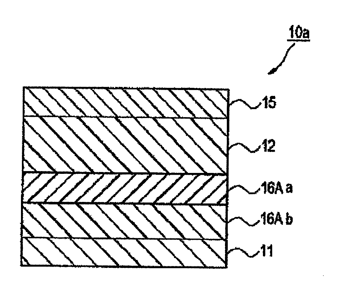
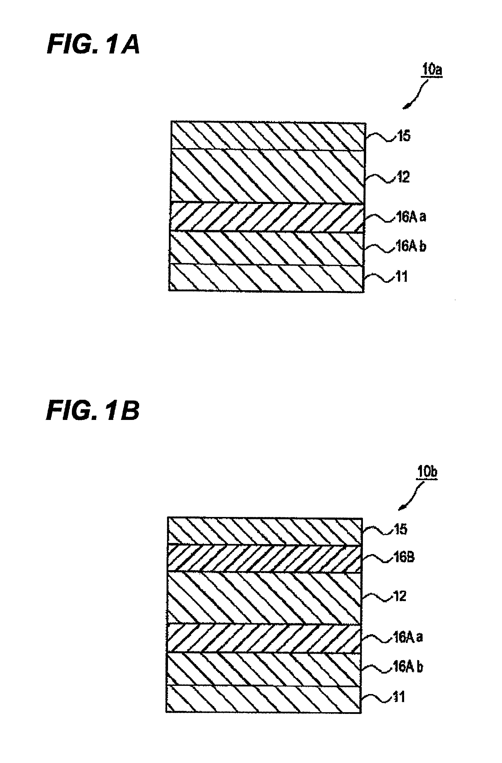
[0191]There is the photoelectric conversion device constituted by the lower electrode / the electron blocking layer 1 / the electron blocking layer 2 (mixed layer) / the photoelectric conversion layer / the upper electrode / the sealing layer, which are sequentially formed. The electron blocking layer 1 is the electron blocking layer in which the content of a fullerene or a fullerene derivative is the volume ratio of 10% or less. The layer in which the electron blocking layer 1 and the mixed layer are mixed is the electron blocking layer. The electron blocking layer 1, the mixed layer, the photoelectric conversion layer, and the upper electrode were sequentially formed on the lower electrode. The lower electrode is TiN. The electron blocking layer 1 was formed in the film thickness of 60 nm by using the organic compound represented by compound 1 by the vacuum deposition method. In the mixed layer, the mixed layer of the organic compound represented by the compound 1 and C60 (compound 1:C60=1:...
examples 2 to 4 , 6 to 8 , 10 to 12 , 14 to 16 , 18 to 20 , 22 to 31
Examples 2 to 4, 6 to 8, 10 to 12, 14 to 16, 18 to 20, 22 to 31
[0193]As shown in Tables 3 to 16, the devices of Examples 2 to 4, 6 to 8, 10 to 12, 14 to 16, 18 to 20, and 22 to 31 were manufactured in the same manner as Example 1 by changing the materials of the electron blocking layer 1, the electron blocking layer 2 (mixed layer), and the photoelectric conversion layer (bulk hetero layer), and the mixing ratio and the film thickness of the materials.
example 5
[0194]There is the photoelectric conversion device constituted by the lower electrode / electron blocking layer 2 (mixed layer) / the photoelectric conversion layer / the upper electrode / the sealing layer, which are sequentially formed. The electron blocking layer 2 (mixed layer), the photoelectric conversion layer, and the upper electrode are formed in this order. The lower electrode is TiN. In the mixed layer, the mixed layer of the organic compound represented by the compound 1 and C60 (compound 1:C60=1:1 (volume ratio)) was formed in the film thickness of 100 nm under the vacuum by the co-deposition. In the photoelectric conversion layer, the mixed layer of the organic compound represented by the compound 2 and C60 (compound 2:C60=1:2 (volume ratio)) was formed in the film thickness of 400 nm under the vacuum by the co-deposition. The upper electrode was formed of ITO in the film thickness of 10 nm by the high frequency magnetron sputter. The sealing layer was formed of the laminate f...
PUM
 Abstract
Description
Claims
Application Information