Method for separating and collecting carbon nanotube, and carbon nanotube

a technology of carbon nanotubes and carbon nanotubes, which is applied in the direction of separation processes, instruments, ion-exchangers, etc., to achieve the effects of accurate separation, high accuracy and automatic separation

Inactive Publication Date: 2014-05-06
NAT INST OF ADVANCED IND SCI & TECH
View PDF17 Cites 12 Cited by
  • Summary
  • Abstract
  • Description
  • Claims
  • Application Information

AI Technical Summary

Benefits of technology

[0044]The present invention enables semiconducting CNTs to be separated by structure simultaneously with the separation of metallic CNTs and semiconducting CNTs. The invention also enables semiconducting CNTs of a specific structure to be separated from a mixture of semiconducting CNTs. The invention is applicable not only to continuous separation using a column, but to batch separation. More than one kind of semiconducting CNTs of specific structures can be obtained at once with high accuracy. In the foregoing technique for separating semiconducting CNTs of a single structure with the use of an expensive synthetic DNA (Non-Patent Document 7), a synthetic DNA of a specific sequence needs to be prepared for the CNTs of each different structure. In contrast, in the present invention, the same reagent may be used for the separation of semiconducting CNTs of each different structure, and the invention is very desirable in terms of ease of operation, and cost. Further, accurate separation is possible with inexpensive equipment, and the columns can be reused. It is also possible to automate the separation. These advantages can greatly reduce separation cost. Further, the method can be said as a very practical method, because it can separate semiconducting CNTs by structure, simultaneously with the separation of metallic CNTs and semiconducting CNTs.

Problems solved by technology

However, all of these reports pose problems in industrial production of metallic CNTs and semiconducting CNTs, as follows.
(1) The separation involves complicated steps, and cannot be automated; (2) the separation is time consuming; (3) mass processing is not possible; (4) expensive equipment and chemicals are required; (5) only one of the metallic CNTs and semiconducting CNTs are obtained; and (6) the collection rate is low.
However, these techniques also have the foregoing problems.
Particularly, the final material is limited to metallic CNTs, and the collection rate is low.
These techniques also have the foregoing problems.
Particularly, the resulting final material is limited to semiconducting CNTs, and the collection rate is low.
This technique is also problematic, because the method uses a very expensive ultracentrifugal separator, and requires a long time for the ultracentrifugal separation procedure.
Further, because the ultracentrifugal separator can only be increased to a certain size, more than one ultracentrifugal separator needs to be installed in parallel, and accordingly automation and other processes are difficult.
A problem of this method, however, is that it requires an expensive synthetic DNA, and that the collection rate and purity are poor because of the moderate separation accuracy.
The method thus inevitably involves strict step control, and does not successfully separate metallic CNTs and semiconducting CNTs (Patent Document 6, Example 4).
Separation of semiconducting CNTs by diameter or structure also involves problems similar to those identified in the separation of metallic CNTs and semiconducting CNTs.
However, the technique has problems as above, including the need to use a very expensive device, a long separation time, limited size, and difficulties in implementing automation and other processes.
However, the method is problematic, because it requires a specific synthetic DNA for the CNTs of each individual structure, and that the synthetic DNA is very expensive.
However, the method suffers from low accuracy in the diameter-specific separation, and requires further improvement for obtaining semiconducting CNTs having a uniform structure.Patent Document 1: JP-A-2007-31238Patent Document 2: JP-A-2005-325020Patent Document 3: JP-A-2005-194180Patent Document 4: JP-A-2005-104750Patent Document 5: JP-A-2006-512276Patent Document 6: JP-A-2005-527455Patent Document 7: JP-A-2004-142972Patent Document 8: JP-A-2006-282418Patent Document 9: JP-A-2008-285386Patent Document 10: JP-A-2008-285387Patent Document 11: WO2009 / 075293Patent Document 12: Japanese Patent Application No. 2009-147557Non-Patent Document 1: Advanced Materials 18, (2006) 1468-1470Non-Patent Document 2: J. Am. Chem. Soc. 127, (2005) 10287-10290Non-Patent Document 3: J. Am. Chem. Soc. 128, (2006) 12239-12242Non-Patent Document 4: J. Phys. Chem. B 110, (2006) 25-29Non-Patent Document 5: Nature Nanotechnology 1, (2006) 60-65Non-Patent Document 6: Nano Letters 9, (2009) 1497-1500Non-Patent Document 7: NATURE 460, (2009) 250-253

Method used


Image

  • Method for separating and collecting carbon nanotube, and carbon nanotube
  • Method for separating and collecting carbon nanotube, and carbon nanotube
  • Method for separating and collecting carbon nanotube, and carbon nanotube

Examples


example 1

[0087]A CNT sample was added in large excess to a column to separate and collect semiconducting CNTs of single chirality.

Preparation of CNT Dispersion

[0088]A 2% SDS aqueous solution (100 ml) was added to 100 mg of Hipco-CNTs (CNI; CNTs synthesized by chemical vapor deposition; diameter 1.0±0.3 nm). The solution was sonicated at a 20 W / cm2 output for 20 hours while being cooled in cold water, using a tip-type ultrasonic homogenizer (Sonifier; Branson; tip diameter 0.5 inches). The dispersion resulting from the sonication was subjected to ultracentrifugal separation (197,000×g, 15 min) to collect 80% of the supernatant. The solution was then used as a CNT dispersion.

Column Preparation and Separation

[0089]Gel beads (Sephacryl S-300; GE healthcare) were used as a column support. The gel beads were charged into a plastic column (length 7.5 cm; inner diameter 1.5 cm) until the height reached about 2 mm, and equilibrated with a 2% SDS aqueous solution after passing deionized water. A CNT d...

example 2

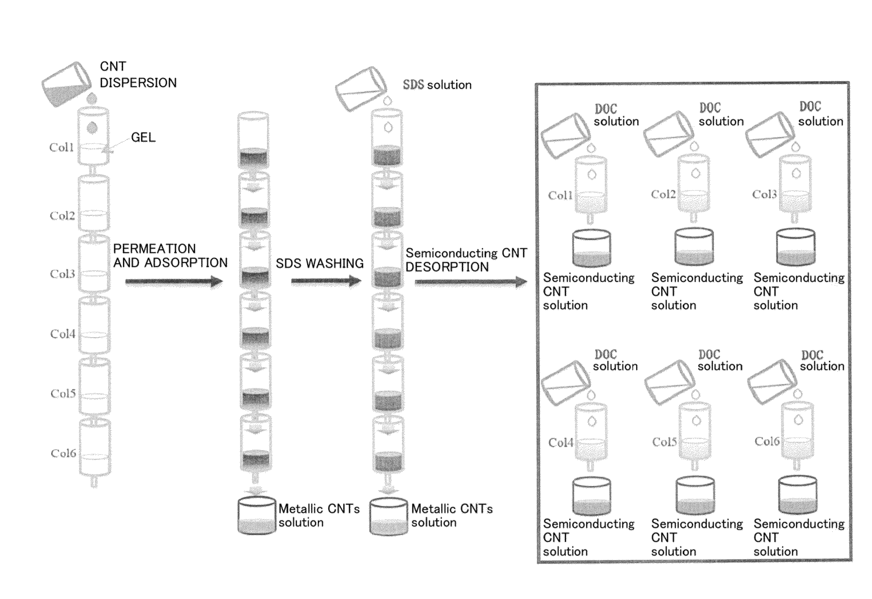
[0093]The same experiment conducted in Example 1 was performed by using a plurality of columns connected in series. CNTs of different chiralities were adsorbed in different columns at once, and, after separating the columns, the CNTs adsorbed in each column were collected to separate and collect the CNTs of different chiralities at once.

Column Preparation and Separation

[0094]As represented in FIG. 1, six columns were connected in series. Sephacryl S-300 that provides desirable purity for the (6,5) CNTs was used for the columns of the first and second stages, though separation is possible with either of Sephacryl S-200 and Sephacryl S-300. Sephacryl S-300 was charged to the height of about 2 mm in the first column, and to the height of about 3.5 mm in the second column. Sephacryl S-200 was used for the third to sixth columns by being charged to the height of about 6 mm. Prior to the separation, the columns were equilibrated with deionized water and a 2% SDS aqueous solution in this o...

example 3

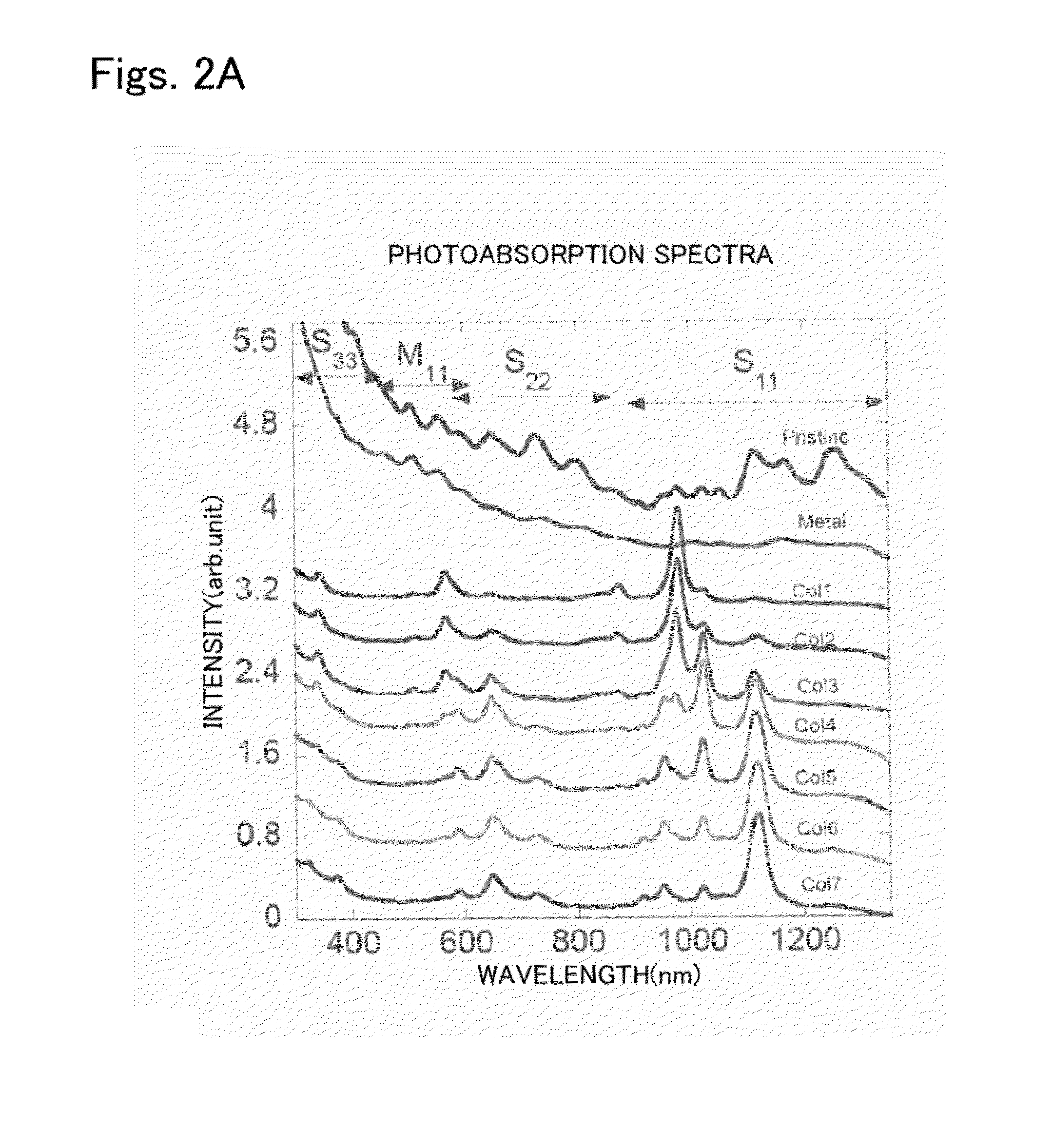
[0104]The same experiment conducted in Example 2 was performed by using different CNTs (CoMoCAT-CNTs, Southwest Nano Technologies; diameter 0.8±0.1 nm). Six columns charged with Sephacryl S-300 were connected in series, and a 10-ml CNT dispersion was added thereto. Two cycles of separation using a 2% SDS aqueous solution as a developing solvent were repeated, and the CNT solution that did not bind to any of the columns was collected as metallic CNTs (Metal). Almost all of the semiconducting CNTs adsorbed with a 2% SDS solution, because the CNTs used in this experiment had small diameters, and were strongly adsorbable by the gel. Accordingly, the third adsorption experiment using a lowered SDS concentration was not conducted. The results of photoabsorption spectral measurement using the CoMoCAT-CNT showed the tendency for CNTs of smaller diameters to adsorb on the columns sooner than the thicker CNTs (FIG. 5). FIG. 6 represents the result of fluorescence spectral measurement. The CoM...


PUM

PropertyMeasurementUnit
concentrationaaaaaaaaaa
absorption wavelengthaaaaaaaaaa

Abstract

Metallic CNTs and semiconducting CNTs are efficiently separated from a CNT mixture of these CNTs, and semiconducting CNTs are separated by structure by using a method that enables separation in high yield in a short time period while conveniently enabling mass processing and automatic processing with inexpensive equipment.Multiple columns charged with gel are connected in series, and excess amounts of a CNT dispersion is passed through the columns to adsorb only the CNTs of a specific structure on the columns. The CNTs are then eluted with an elution to separate CNTs of different structures with high accuracy. The present technique represents a method that conveniently enables mass processing and automatic processing at high yield in a short time period with inexpensive equipment.

Description

TECHNICAL FIELD[0001]The present invention relates to a method for efficiently separating metallic carbon nanotubes and semiconducting carbon nanotubes from carbon nanotubes (CNTs) containing these carbon nanotubes, and for separating the semiconducting CNTs by structure. The present invention also relates to carbon nanotubes obtained by using the method.BACKGROUND ART[0002]CNTs have excellent electrical characteristics and mechanical strength along with other superior properties, and have been actively researched and developed as an ultimate novel material. CNTs are synthesized by using various methods, including a laser vaporization method, an arc discharge method, and a chemical vapor deposition method (CVD method). However, CNTs produced by using any of the currently available synthesis methods are obtained as a mixture of metallic CNTs and semiconducting CNTs.[0003]Because either one of the metallic and semiconducting properties is often used in actual use, separation and purif...

Claims


Application Information

Patent Timeline
Patent Type & Authority Patents(United States)
IPC IPC(8): D01F9/12G01N30/02B82Y40/00B82Y30/00
CPCB82Y40/00B82Y30/00C01B2202/22C01B31/0266G01N30/461G01N2030/8863C01B32/172C01B32/17
Inventor LIU, HUAPINGTANAKA, TAKESHIKATAURA, HIROMICHI
Owner NAT INST OF ADVANCED IND SCI & TECH
Why Eureka
Try Eureka