Oscillator having negative resistance element

a resistance element and oscillator technology, applied in the field of oscillators, can solve the problems of limiting the improvement of power conversion efficiency, and achieve the effect of reducing the service life and the gain of the elemen

Active Publication Date: 2014-07-15
CANON KK
View PDF42 Cites 9 Cited by
  • Summary
  • Abstract
  • Description
  • Claims
  • Application Information

AI Technical Summary

Benefits of technology

[0008]With the method of PTL 1, the negative resistance is cancelled in a low frequency region so as not to generate any gain and suppress any parasitic oscillation by replacing diode element 63 with a resistance element whose resistance is substantially same as the negative resistance of the RTD element 64 of FIG. 6. The low frequency as used herein is substantially of the order of kHz and MHz, although it may vary depending on the length of the cable for connecting the power bias circuit to the RTD element. However, the resistance value of a resistance element as described above is about tens of several ohms (Ω) and a DC current that does not participate in oscillation flows to the resistance element to provide a limit to improvement of power conversion efficiency. On the other hand, NPL 1 employs a diode element 63 to replace a resistance element as described above. Any parasitic oscillation is prevented from appearing by selecting a differential resistance value that can cancel the negative resistance for the diode element 63 near the bias voltage when the RTD element is driven to oscillate. With such an arrangement again, a DC current is made to flow to an element other than the RTD element to provide a limit to reduction of power consumption.
[0009]Furthermore, both a resistance element and a diode element emit heat to consume electric power as an electric current is made to flow to them. Then, as a result, the RTD element is heated as heat emitting members are integrally arranged near the RTD element to reduce the service life and the gain of the element.

Problems solved by technology

However, the resistance value of a resistance element as described above is about tens of several ohms (Ω) and a DC current that does not participate in oscillation flows to the resistance element to provide a limit to improvement of power conversion efficiency.
Furthermore, both a resistance element and a diode element emit heat to consume electric power as an electric current is made to flow to them.

Method used


Image

  • Oscillator having negative resistance element
  • Oscillator having negative resistance element
  • Oscillator having negative resistance element

Examples


embodiment 1

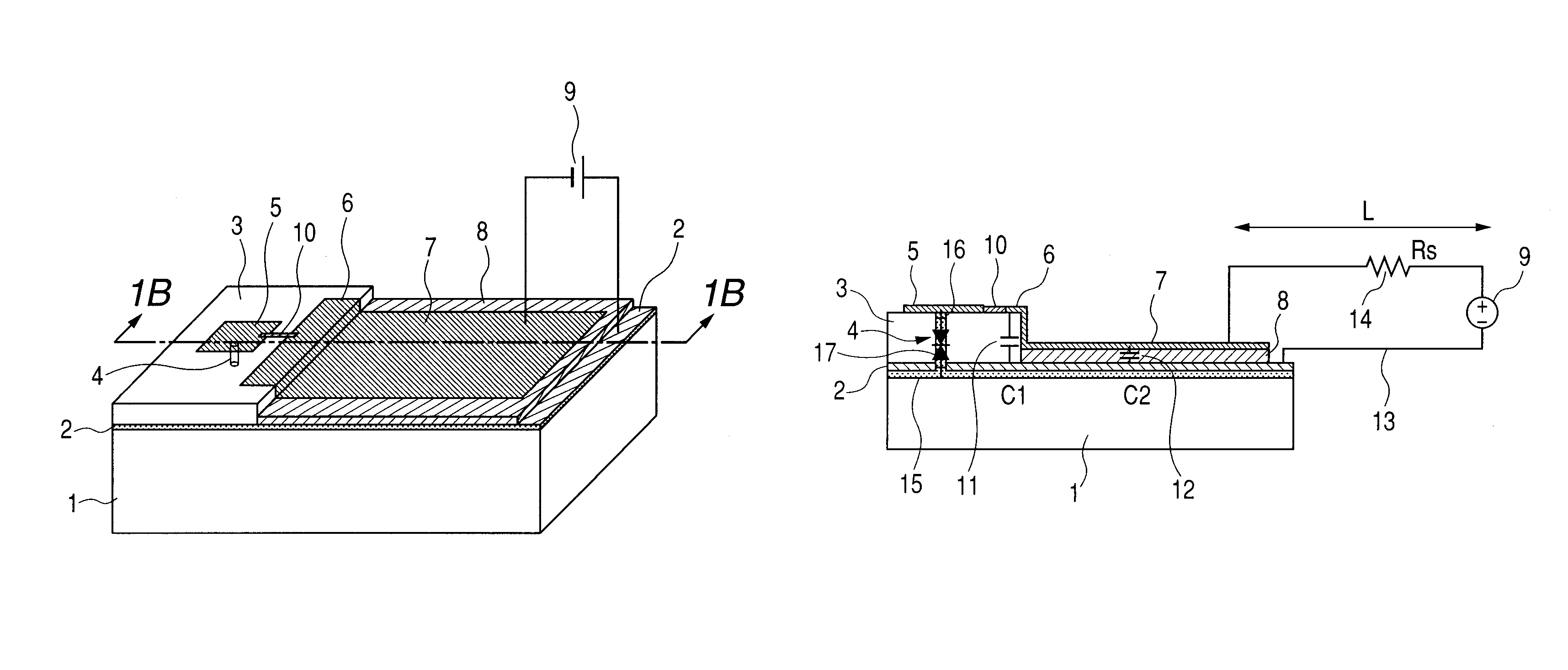
[0023]Embodiment 1 of the present invention has a structure formed by integrating an RTD element and a large capacitance capacitor on a same substrate. FIGS. 1A and 1B illustrate the structure thereof, of which FIG. 1A is a schematic perspective view and FIG. 1B is a schematic cross-sectional view taken along 1B-1B in FIG. 1A. In FIGS. 1A and 1B, 4 denotes a post-shaped RTD element and the structure further includes epitaxial layers including an InGaAs / AlAs or InGaAs / InAlAs quantum well 17, a pair of contact layers 15, 16 and spacer layers (not illustrated) formed on an InP substrate 1 by crystal growth thereof. A negative resistance element formed by using a III-V group compound semiconductor such as AlGaAs / GaAs on a GaAs substrate and AlGaN / InGaN on a GaN substrate, a IV group semiconductor such as Si / SiGe on an Si substrate, and a II-VI group semiconductor may also be applicable.

[0024]The resonator is formed by an electrode 2 that also operates as a ground plane, an electrode 5 t...

example 1

[0036]A specific example of arrangement of elements of Embodiment 1 will be described below. In this example, an RTD element is formed on an InP substrate. A triple barrier quantum well structure having a first barrier layer AlAs (1.3 nm), a first quantum well layer InGaAs (7.6 nm), a second barrier layer InAlAs (2.6 nm), a second quantum well layer InGaAs (5.6 nm), a third barrier layer AlAs (1.3 nm) is employed. All the composition ratios are lattice-matched to the InP substrate except AlAs. On the other hand, AlAs is a strained layer but the thickness is less than the critical film thickness. A spacer layer made of non-doped InGaAs, an n-type InGaAs electric contact layer and an n+InGaAs contact layer are arranged at the top and also at the bottom of the triple barrier quantum well structure. The RTD element post is circular with a diameter of about 2 μm. Then, current voltage characteristics including a current density of Jp=280 kA / cm2, a peak valley ratio of 3 and a differentia...

embodiment 2

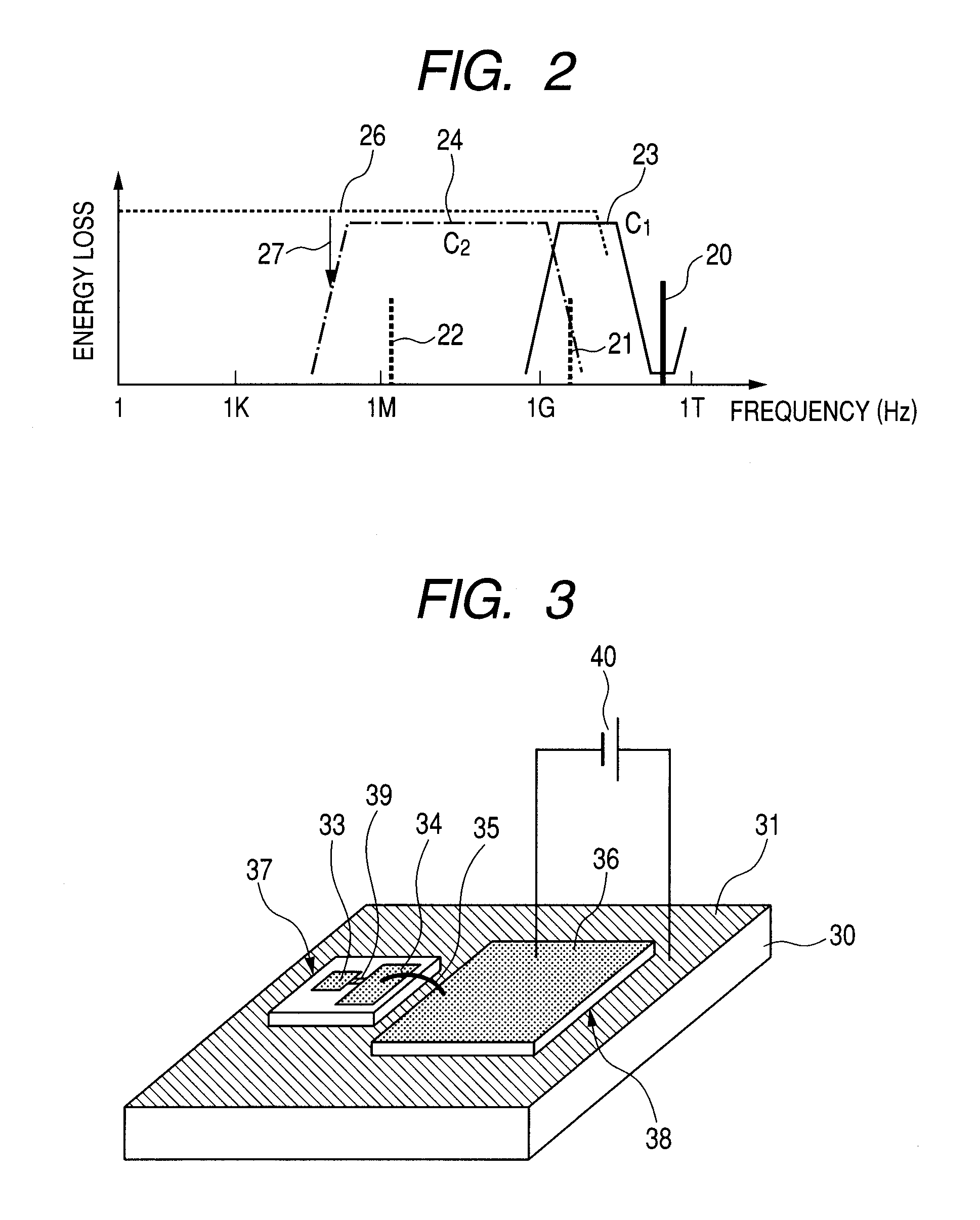
[0038]Embodiment 2 of the present invention has such a structure that a second capacitor is installed on a same mount as a separate chip as illustrated in FIG. 3. In FIG. 3, 30 denotes a sub-carrier for installing the chips. A substrate prepared by coating an electroconductive layer 31 such as Au on a ceramic substrate such as Si substrate, Al2O3 and AlN or on a plastic substrate or a metal plate may selectively be employed for the sub-carrier 30. 37 denotes an RTD element chip or a single chip realized to carry the RTD element and components down to the part that corresponds to the first capacitor of Embodiment 1. A patch antenna 33 and an electrode 34 are connected by a line 39. Note, however, that the capacitance of the part that corresponds to the first capacitor needs to be made larger than that of Embodiment 1. One of the contacts of the RTD element is connected to the electroconductive layer 31 of the sub-carrier and the other contact is connected to one of the electrodes (36...


PUM


Abstract

An oscillator has a negative resistance element and a resonator along with a capacitor electrically connected in parallel with the negative resistance element relative to a power bias circuit, a capacitance of the capacitor being so selected as to suppress any parasitic oscillation due to the power bias circuit and allow oscillation at a resonance frequency due to the negative resistance element and the resonator.

Description

TECHNICAL FIELD[0001]The present invention relates to an oscillator and, more particularly, to a current injection type oscillator oscillating an electromagnetic wave including at least a part thereof a frequency component in a frequency region from the millimeter wave band to the terahertz wave band (more than 30 GHz and not more than 30 THz). More detailedly, the present invention relates to a current injection type oscillator having a negative resistance element such as an element having a resonant tunneling diode structure.BACKGROUND ART[0002]Non-destructive sensing techniques using electromagnetic waves in a frequency region from the millimeter wave band to the terahertz wave band (more than 30 GHz and not more than 30 THz) have been developed. Fields of application of electromagnetic waves of the frequency bands cover imaging techniques using safe fluoroscopic examination apparatus that replace X-ray apparatus. Techniques such as a spectroscopic technique of examining physical...

Claims


Application Information

Patent Timeline
Patent Type & Authority Patents(United States)
IPC IPC(8): H03B7/14
CPCH03B9/12H03B7/08
Inventor OUCHI, TOSHIHIKOSEKIGUCHI, RYOTA
Owner CANON KK
Why Eureka
Try Eureka