Seed light generation device, light source device, adjustment method thereof, light irradiation device, exposure device, and device manufacturing method
a light source device and seed technology, applied in the field of seed light generation devices, can solve the problems of reducing the transfer accuracy of mask patterns, generating problems due to this increase in spectral width, deteriorating the image forming characteristic of projection optical systems, etc., and reducing the spectral width of the output of light source devices. , the effect of seed light not being generated
- Summary
- Abstract
- Description
- Claims
- Application Information
AI Technical Summary
Benefits of technology
Problems solved by technology
Method used
Image
Examples
first embodiment
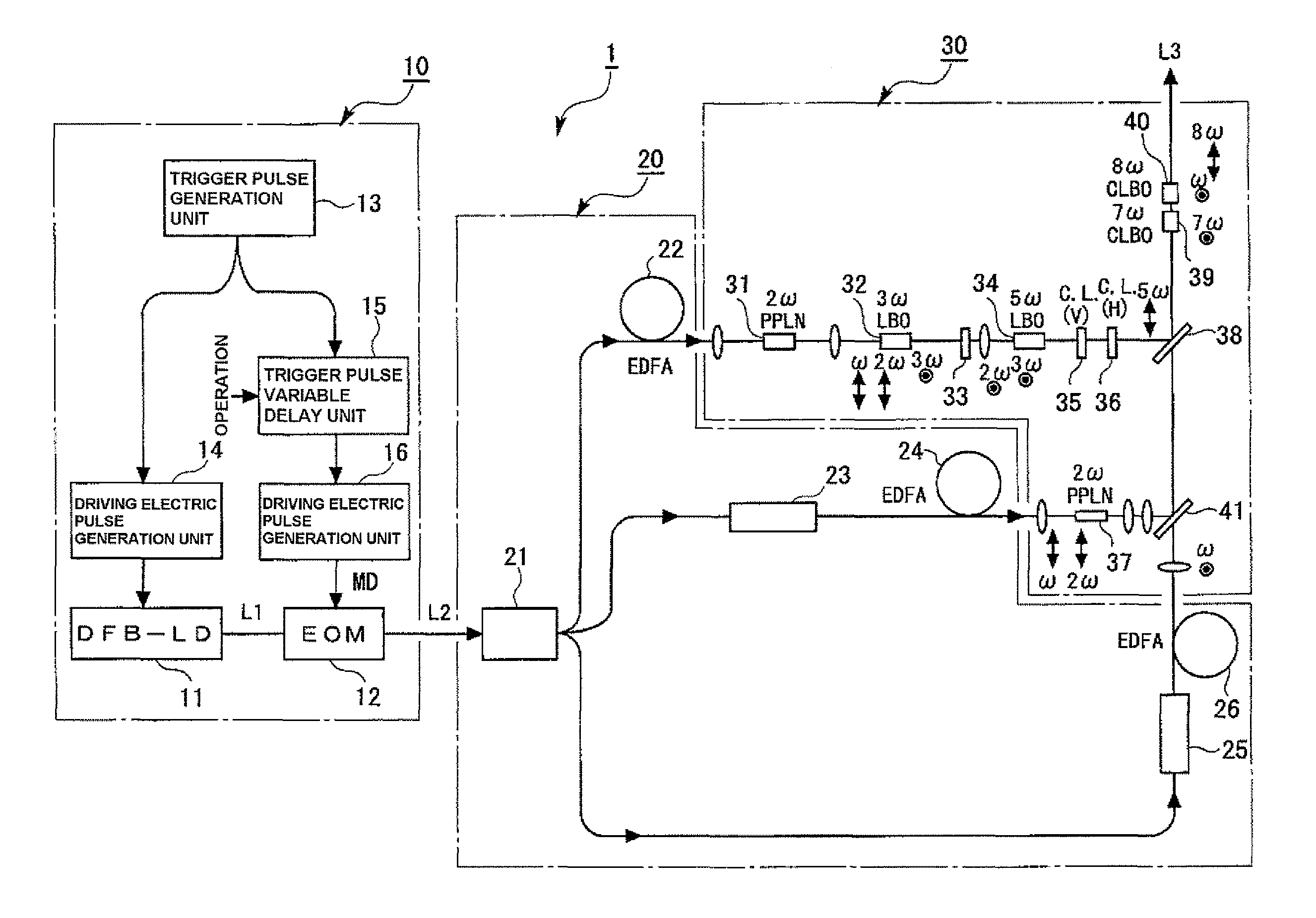
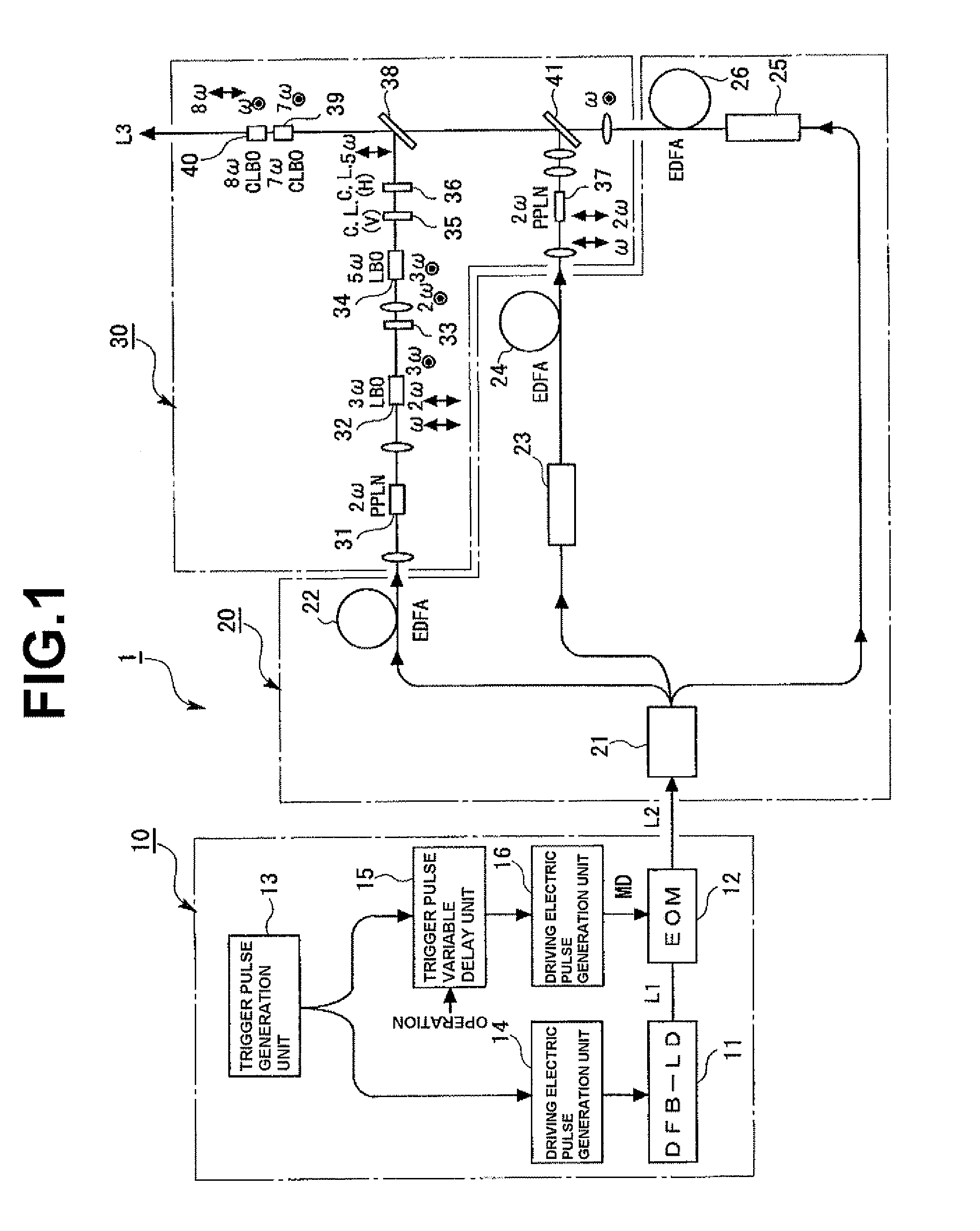
[0030]FIG. 1 is a diagram depicting a general configuration of a light source device 1 according to a first embodiment of the present invention. The light source device 1 according to the present embodiment has a seed light generation device 10 which generates seed light L2 to be optically amplified, a light amplification unit 20 which optically amplifies the seed light L2 generated by the seed light generation device 10, and a wavelength conversion unit 30 which converts the wavelength of the light optically amplified by the light amplification unit 20, and outputs ultraviolet pulsed light having a 193 nm wavelength as light source light (output light of the wavelength conversion unit 30) L3.
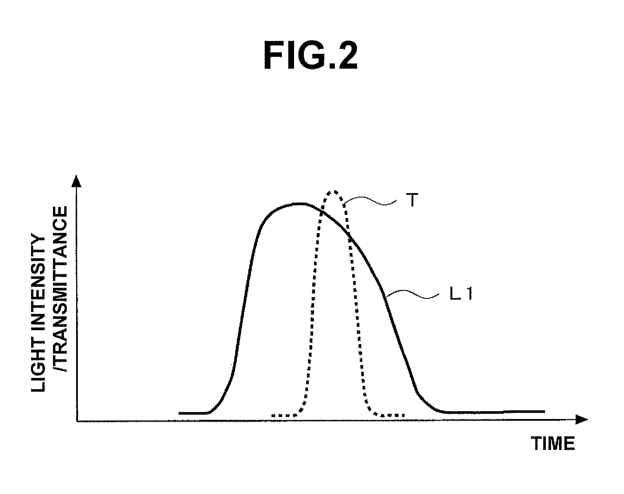
[0031]According to the present embodiment, the seed light generation device 10 has: a distributed feedback laser diode (DFB-LD) 11 as a pulse generation unit for generating pulsed light L1 having a single wavelength, in an infrared or visible range; an electro-optic modulator (EOM) 12 as a puls...
second embodiment
[0062]FIG. 6 is a diagram depicting a general configuration of an exposure device 50 according to a second embodiment of the present invention. The exposure device 50 according to this embodiment is constituted by the light source device 1 of the first embodiment, and is used for a photolithography step, which is one of the semiconductor manufacturing steps. The exposure device used for the photolithography step is theoretically the same as photo-engraving, where a device pattern (mask pattern), accurately drawn on a photomask (reticle), is optically projected and transferred onto a semiconductor wafer, glass substrate or the like on which photoresist is coated.
[0063]The exposure device 50 according to this embodiment has: the above-mentioned light source device 1; an irradiation optical system (illumination optical system) 51; a mask support 53 for supporting a photomask (reticle) 52; a projection optical system 54, a stage 56 which mounts and supports a semiconductor wafer 55 as a...
PUM
| Property | Measurement | Unit |
|---|---|---|
| light transmittance | aaaaa | aaaaa |
| wavelength | aaaaa | aaaaa |
| oscillation wavelength | aaaaa | aaaaa |
Abstract
Description
Claims
Application Information


