Method of manufacturing semiconductor device

a manufacturing method and technology of semiconductor devices, applied in the direction of manufacturing tools, lapping machines, abrasive surface conditioning devices, etc., can solve the problems of air gap portion shear damage, surface damage of to-be-processed film, etc., and achieve the reduction of yield and reliability of the device, and the number of scratches on the surface of to-be-processed film 13

Active Publication Date: 2014-10-28
KIOXIA CORP
View PDF9 Cites 1 Cited by
  • Summary
  • Abstract
  • Description
  • Claims
  • Application Information

AI Technical Summary

Benefits of technology

[0101]According to the first CMP method, the surface of the polishing pad 21 is conditioned at a high temperature within the range of 40° C. or more to 80° C. or leas by supplying the water vapor onto the surface of the polishing pad 21. Thereafter, the to-be-processed film 13 is polished by bringing the surface of the to-be-processed film 13 into contact with the surface of the polishing pad 21 having being conditioned. In this way, the following effect can be obtained.
[0102]The Rsk value of the surface of the polishing pad 21 can be made a negative value having a larger absolute value by conditioning the surface of the polishing pad 21 at a higher temperature. The number of scratches on the surface of the to-be-processed film 13 can be reduced after the CMP process by polishing the to-be-processed film 13 by bringing the surface of the to-be-processed film 13 into contact with the surface of the polishing pad 21 provided with the negative Rsk value. As a result, a reduction in yield and reliability of the device can be suppressed.
[0103]Next, a second CMP method will be explained using FIGS. 11 and 15. Note that, in the second CMP method, an explanation of the same points as those of the first CMP method is omitted, and different points will be mainly explained.
[0104]A CMP device in the second CMP method will be explained below using FIG. 15.
[0105]FIG. 15 is a configuration view showing the CMP device in the second CMP method.
[0106]As shown in FIG. 15, the CMP device in the second CMP method is different from that of the first CMP method in that a heater 28 is provided in place of the vapor supply nozzles 27.

Problems solved by technology

Because of this, after the CMP process, the surface of the to-be-processed film is damaged (scratched) by polishing executed using the abrasive grains.
For this reason, when a surface of the to-be-processed film on the air gap is planarized by the CMP technology, an air gap portion is shear damaged (cracked) by a shearing stress at the time of the CMP process in addition to the generation of the scratches.

Method used


Image

  • Method of manufacturing semiconductor device
  • Method of manufacturing semiconductor device
  • Method of manufacturing semiconductor device

Examples


embodiments

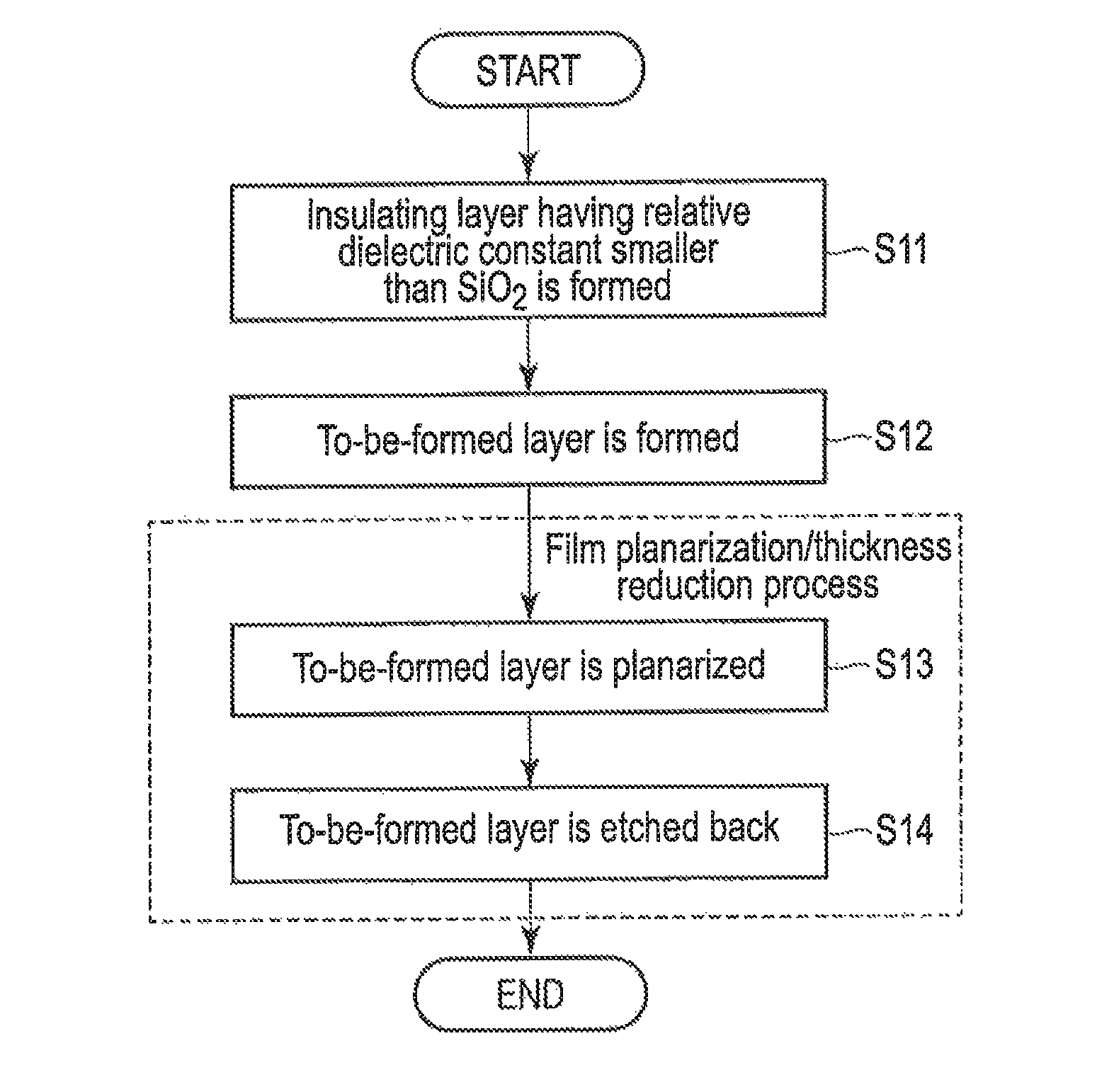
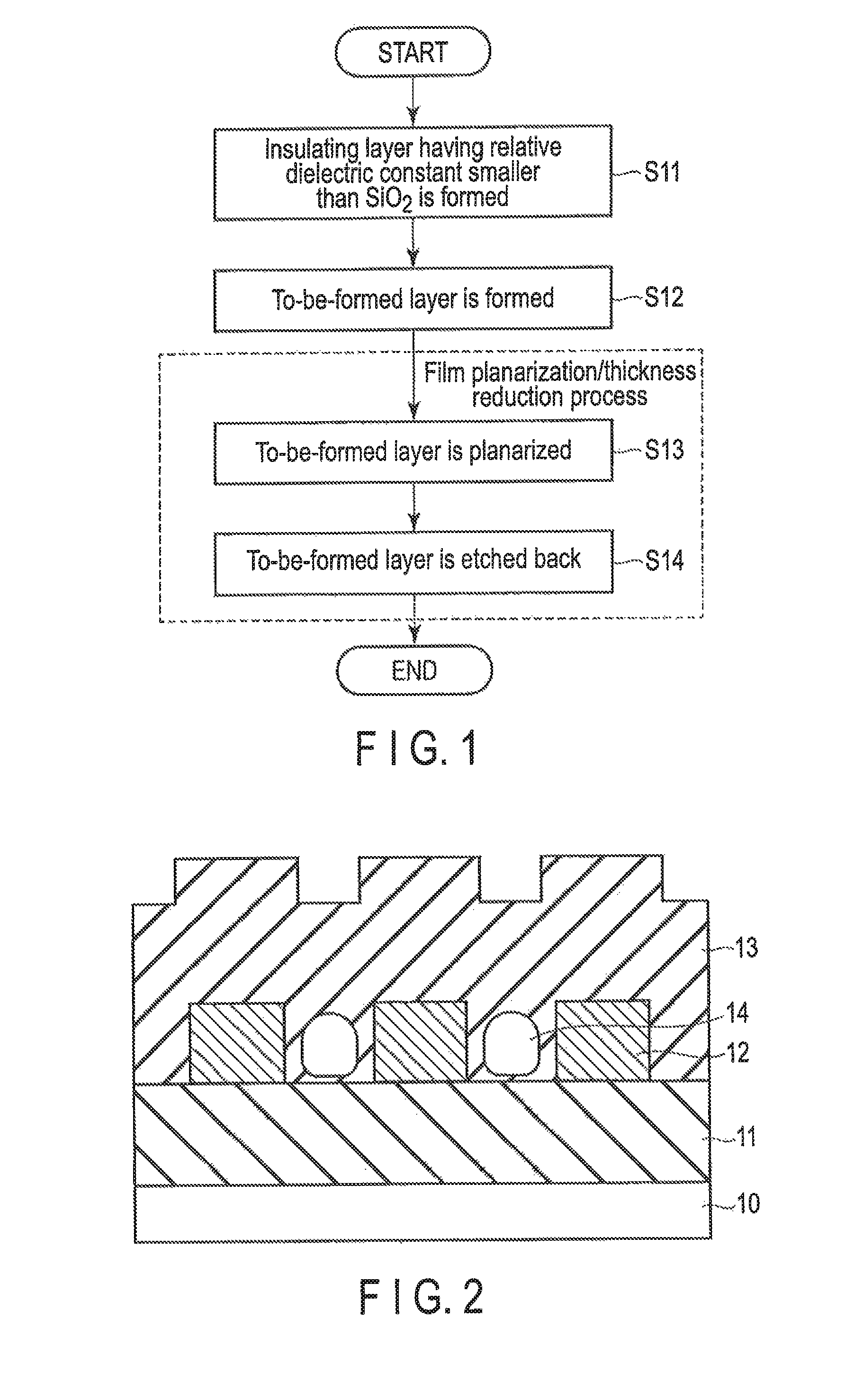
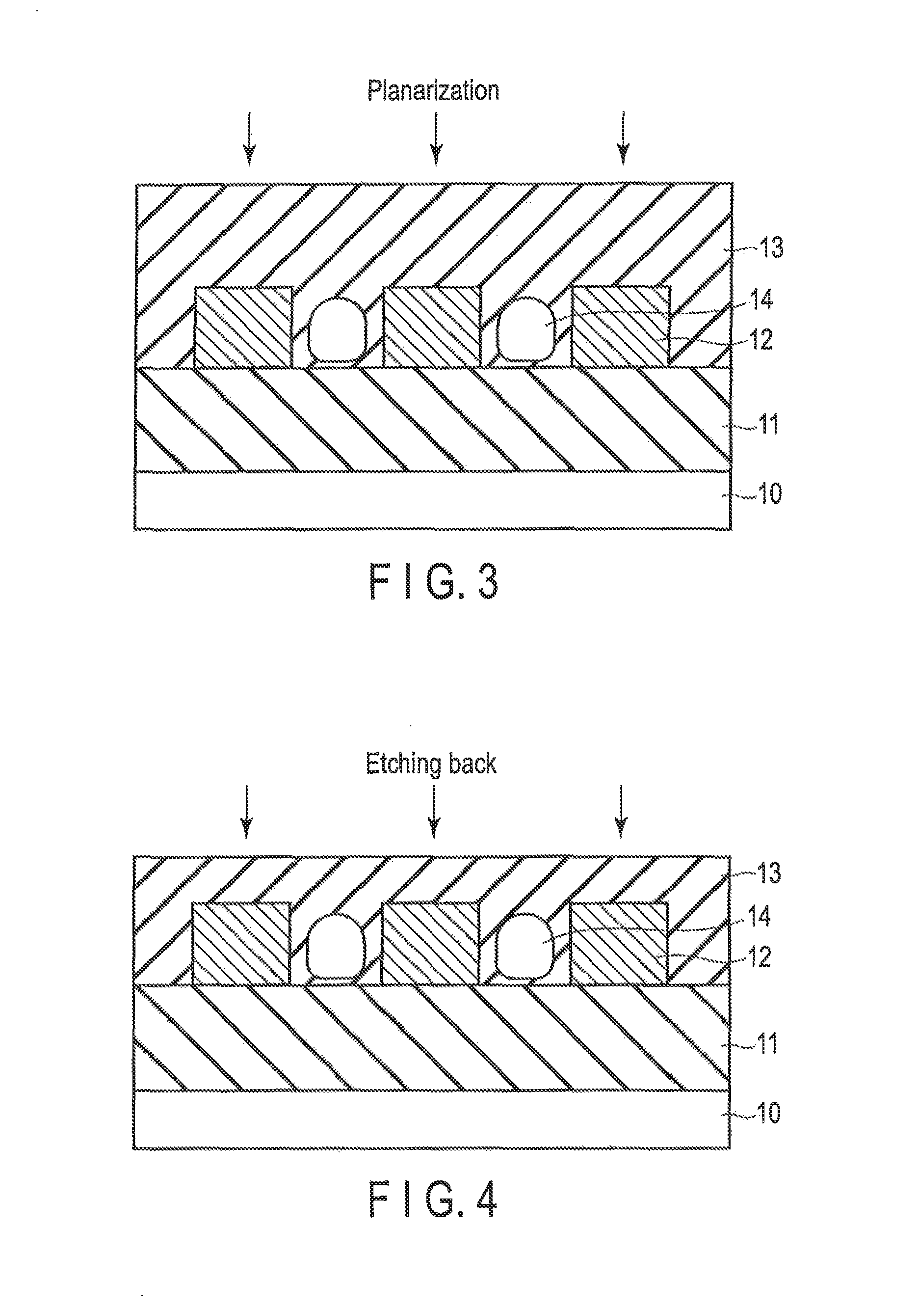
[0029]Embodiments will be explained using FIGS. 1 to 27. The embodiments are a film planarization / thickness reduction method of a to-be-processed film 13 which is formed on an insulation layer (for example, an air gap 14 or a porous layer 15) that has a relative dielectric constant smaller than that of silicon oxide (SiO2) and a low mechanical strength. More specifically, the film planarization / thickness reduction method has a step of planarizing the to-be-processed film 13 having a convex potion and concave potion on the air gap 14 or the porous layer 15 by a predetermined planarization method and a step of thinning the to-be-processed film 13 by etching back the to-be-processed film 13. With these steps, a desired flatness can be obtained while suppressing scratches and cracks generated to the to-be-processed film 13. The embodiments will be explained below in detail.

[1. Method of Manufacturing Semiconductor Device According to Embodiment]

[0030]A manufacturing method of a semicond...

first example

[0176]FIGS. 23A to 23D are sectional views showing flows in a first example according to the first chemical polishing method and are sectional views showing a to-be-processed film 13 having an irregularity 31.

[0177]As shown in FIG. 23A, the to-be-processed film 13 has the irregularity 31 on its surface. The irregularity 31 has a convex portion 31a and a concave portion 31b. The distance between a surface of the convex portion 31a and a surface of the concave portion 31b (the depth h1 of the irregularity 31) is, for example, about 30 nm or more to 5000 nm or less.

[0178]As shown in FIG. 23B, a surfactant adsorbs onto the to-be-processed film 13 as a surface layer 32. The surfactant (surface layer 32) adsorbed onto the surface of the to-be-processed film 13 acts as a surface protection film. As the surfactant, an anionic surfactant, a cationic surfactant, an amphoteric surfactant and a non-ionic surfactant can be used. Furthermore, the surfactant can be selected among surfactants of an...

second example

[0184]In a second example, as a surface layer 32, polyvinyl pyrrolidone (PVP) that is a cationic surfactant is formed on the surface of the to-be-processed film 13 made of SiO2 (refer to FIG. 23C). In the second example, since the cationic surfactant is used, the surface layer 32 easily adsorbs onto the to-be-processed film 13 made of SiO2 the surface charge of which is negative, and thus the surface layer 32 can be formed easily. In addition to the above mentioned, as a cationic surfactant, polyethyleneimine (PEI) can also be used.

[0185]The weight average molecular weight (Mw) in terms of polyethylene glycol of PVP used in the second example, measured by water-based GPC (gel permeation chromatography) is 20,000 or more, preferably, 200,000 or more to 1,500,000 or less, and more preferably, 300,000 or more to 1,500,000 or less. If the weight average molecular weight is within the above ranges, friction due to contact with a processing body 34 made of a urethane resin can be reduced....


PUM


Abstract

According to one embodiment, a manufacturing method of a semiconductor device comprises forming a to-be-processed film includes a convex potion and concave potion on its surface on a semiconductor substrate via layers having a relative dielectric constant smaller than that of SiO2, planarizing the surface of the to-be-processed film, and etching the planarized surface of the to-be-processed film.

Description

CROSS-REFERENCE TO RELATED APPLICATIONS[0001]This application is based upon and claims the benefit of priority from Japanese Patent Application No. 2013-057178, filed Mar. 19, 2013, the entire contents of which are incorporated heroin by reference.FIELD[0002]Embodiments described herein relate generally to a manufacturing method of a semiconductor device.BACKGROUND[0003]In a manufacturing process of a semiconductor device, there is a CMP (Chemical Mechanical Polishing) technology as a planarization technology of a film surface. In the CMP process, for example, silicon oxide (SiO2) and the like formed on a semiconductor substrate are used as a to-be-processed film and the surface of the film is planarized.[0004]However, in the CMP process, a slurry containing abrasive grains is used. Because of this, after the CMP process, the surface of the to-be-processed film is damaged (scratched) by polishing executed using the abrasive grains.[0005]In contrast, recently, in a semiconductor memo...

Claims


Application Information

Patent Timeline
Patent Type & Authority Patents(United States)
IPC IPC(8): H01L21/306H01L21/302H01L21/461
CPCB24B37/042H01L21/31055B24D5/165B24B53/017B24D5/12H01L21/30625H01L21/31053H01L21/7682H01L21/7684
Inventor MATSUI, YUKITERUGAWASE, AKIFUMIMINAMIHABA, GAKU
Owner KIOXIA CORP
Why Eureka
Try Eureka