Substrate for mounting semiconductor chip and method for producing same

a semiconductor chip and substrate technology, applied in the direction of semiconductor/solid-state device details, printed element electric connection formation, conductive pattern formation, etc., can solve the problem of becoming difficult to secure the wiring for forming electrolytic gold plating on the connecting terminal surface, and achieve excellent wire bondability and solder connection reliability, good conductive effect, and good conductive

Inactive Publication Date: 2015-04-07
RESONAC CORPORATION
View PDF54 Cites 7 Cited by
  • Summary
  • Abstract
  • Description
  • Claims
  • Application Information

AI Technical Summary

Benefits of technology

[0043]According to the invention it is possible to provide a method for producing a substrate for mounting a semiconductor chip, that can reduce bridging and allows excellent wire bondability and solder connection reliability to be obtained, even when forming fine-pitch wirings.
[0044]In addition, since the gold layer can be formed by electroless gold plating in the conductor circuit according to the invention, there is no need to use a lead wire as for electrolytic plating, and it is possible to accomplish satisfactory gold plating on sections that are to serve as independent terminals, even when forming fine-pitch wirings. The production method of the invention can therefore be applied for further micronized and higher density substrates for mounting semiconductor chips.
[0045]Moreover, according to the invention it is possible to provide a method for producing a substrate for mounting a semiconductor chip, that can be obtained by the production method of the invention described above, and that can reduce bridging and allows excellent wire bondability and solder connection reliability to be obtained.

Problems solved by technology

However, with the recent increase in high density of wirings due to smaller substrates for mounting semiconductor chips, it is becoming difficult to secure the wirings for forming electrolytic gold plating on connecting terminal surfaces.

Method used


Image

  • Substrate for mounting semiconductor chip and method for producing same
  • Substrate for mounting semiconductor chip and method for producing same
  • Substrate for mounting semiconductor chip and method for producing same

Examples


first embodiment

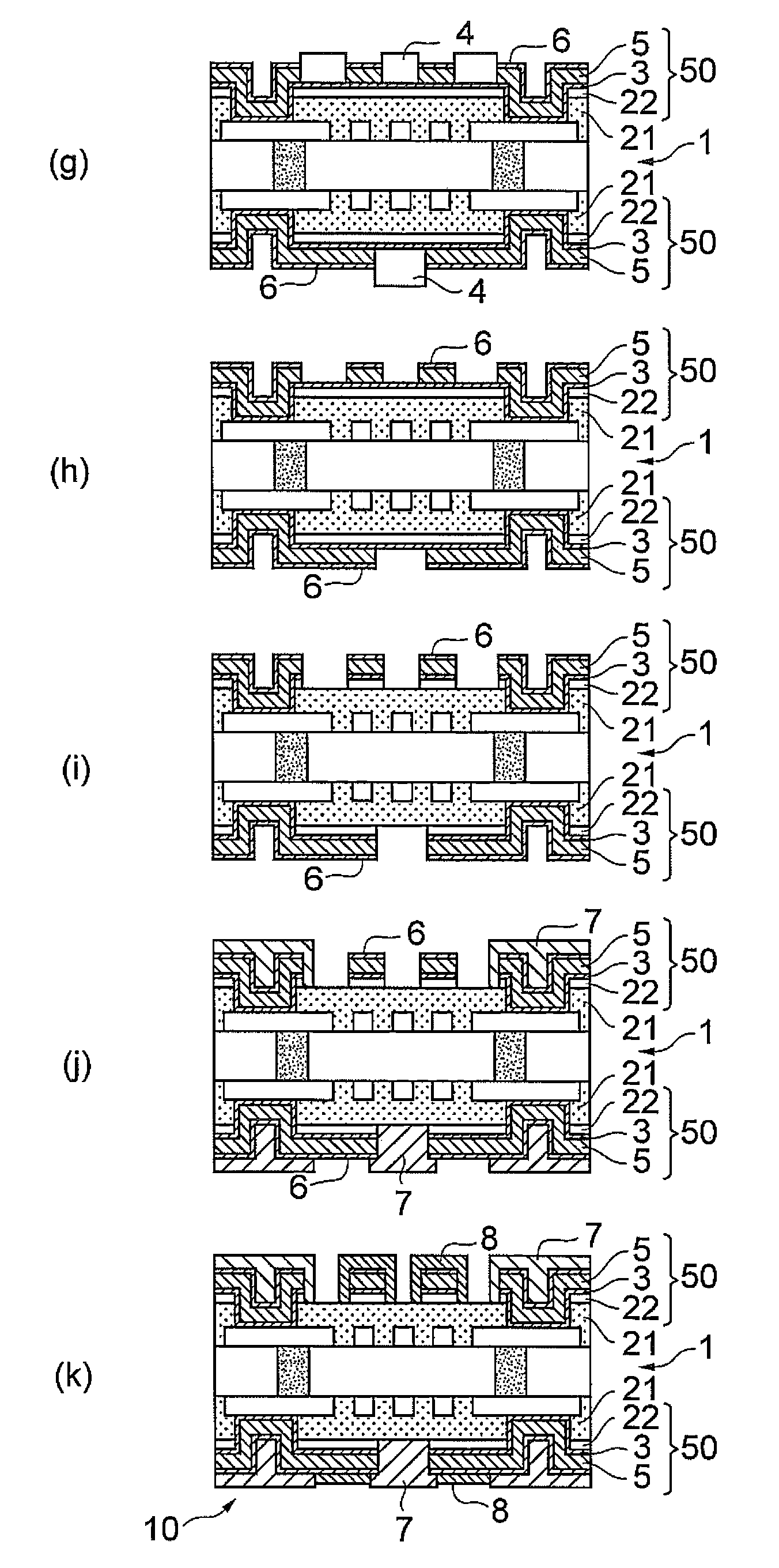
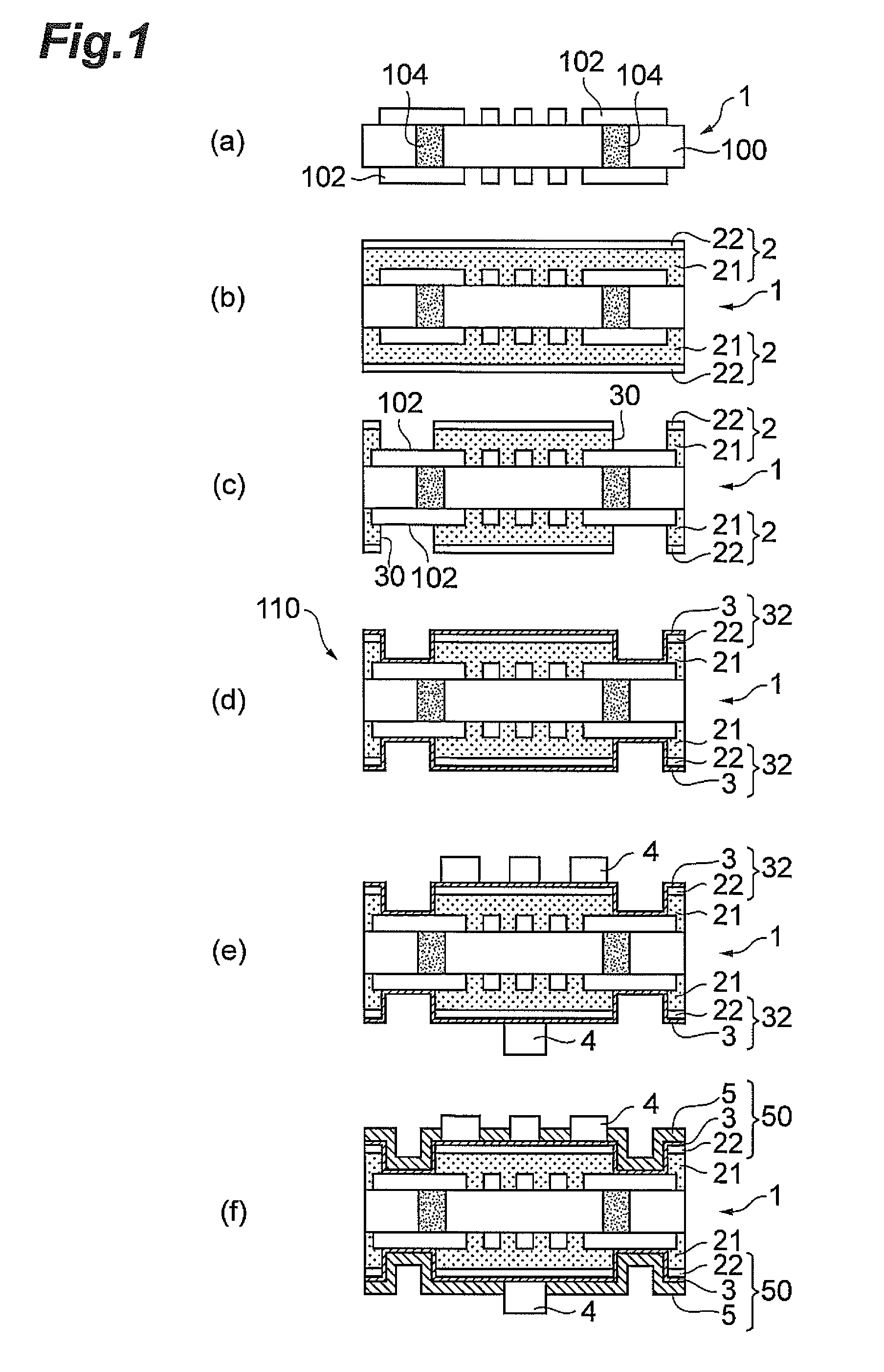
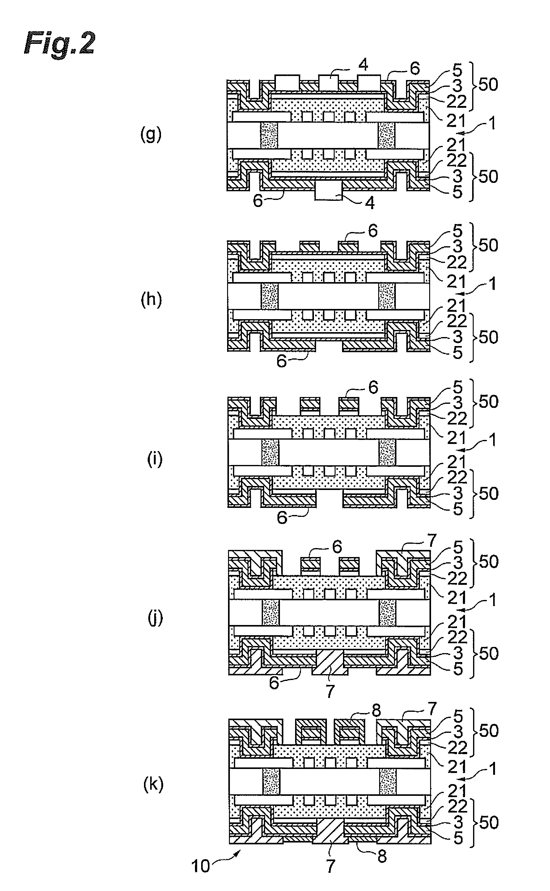
[0061]A preferred first embodiment of a method for producing a substrate for mounting a semiconductor chip will now be explained.FIGS. 1 and 2 are process drawings schematically illustrating the method for producing a substrate for mounting a semiconductor chip according to a first embodiment. This embodiment is an example of a method for producing a substrate for mounting a semiconductor chip by a semi-additive process, wherein an outer layer circuit is formed on an inner board using a copper foil-coated resin.

[0062]According to this embodiment, an inner board 1 is prepared first, as shown in FIG. 1(a). The inner board 1 comprises an inner layer substrate 100, inner layer circuits 102 formed on its surface, and inner layer vias 104 formed through the inner layer substrate and electrically connecting the inner layer circuits 102 on both surfaces. The structures used for the inner board 1 may be known structures applied for circuit boards, without any particular restrictions.

[0063]Th...

second embodiment

[0123]A preferred second embodiment of a method for producing a substrate for mounting a semiconductor chip will now be explained. FIGS. 6 and 7 are process drawings schematically illustrating the method for producing a substrate for mounting a semiconductor chip according to the second embodiment. This embodiment is an example of a method for producing a substrate for mounting a semiconductor chip by a semi-additive process which comprises a step of forming a copper plating layer after a build-up film has been laminated on an inner board.

[0124]According to this embodiment, an inner board 1 is prepared first, as shown in FIG. 6(a). The inner board 1 may be prepared in the same manner as the first embodiment described above. Next, as shown in FIG. 6(b), a build-up film is laminated onto both surfaces of the inner board 1 by lamination or pressing, to form insulating layers 15. The build-up film is a non-conductive film, and comprises an insulating resin material. Such a resin materia...

example 1

Production of Substrate for Mounting a Semiconductor Chip

[0157](1a) Preparation of Inner Board

[0158]First, as shown in FIG. 1(a), an MCL-E-679 (trade name of Hitachi Chemical Co., Ltd.) was prepared as a 0.2 mm-thick glass cloth base material / epoxy copper-clad laminate, having a 18 μm-thick copper foil laminated on both sides of an insulating base material, and the unwanted sections of the copper foil were removed by etching and through-holes were formed, to obtain an inner board with an inner layer circuit formed on the surface (inner board 1).

[0159](1b) Lamination of Resin-Coated Copper Foil

[0160]As shown in FIG. 1(b), MCF-7000LX (trade name of Hitachi Chemical Co., Ltd.) comprising a 3 μm-thick copper foil 22 coated with an adhesive (insulating layer 21) was laminated onto both sides of the inner board by hot pressure for 60 minutes under conditions of 170° C., 30 kgf / cm2.

[0161](1c) Formation of IVH

[0162]As shown in FIG. 1(c), an L-500 Carbon dioxide gas impact laser punching mac...


PUM

PropertyMeasurementUnit
average crystal grain sizeaaaaaaaaaa
thicknessaaaaaaaaaa
thicknessaaaaaaaaaa

Abstract

It is an object of the invention to provide a method for producing a substrate for mounting a semiconductor chip, that can reduce bridging and allows excellent wire bondability and solder connection reliability to be obtained, even when forming fine-pitch wirings. The method for producing a substrate for mounting a semiconductor chip according to the invention comprises a resist-forming step in which a resist is formed on the first copper layer of a stack comprising an inner board with an inner layer circuit on the surface and a first copper layer formed on the inner board separated by an insulating layer at the sections other than those that are to constitute a conductor circuit, a conductor circuit-forming step in which a second copper layer is formed by electrolytic copper plating on the first copper layer to obtain a conductor circuit, a nickel layer-forming step in which a nickel layer is formed by electrolytic nickel plating on at least part of the conductor circuit, a resist removal step in which the resist is removed, an etching step in which the first copper layer is removed by etching, and a gold layer-forming step in which a gold layer is formed by electroless gold plating on at least part of the conductor circuit.

Description

[0001]This is a National Phase Application in the United States of International Patent Application No. PCT / JP2010 / 065229 filed Sep. 6, 2010, which claims priority on Japanese Patent Application No. P2009-205856, filed Sep. 7, 2009. The entire disclosures of the above patent applications are hereby incorporated by reference.TECHNICAL FIELD[0002]The present invention relates to a substrate for mounting a semiconductor chip and to a method for producing it.BACKGROUND ART[0003]In recent years, continuing advancements have been made in size and weight reduction, high performance and high functionality of electronic devices such as personal computers, cellular phones, wireless base stations, optical communication devices, servers and routers, of various sizes. With the increasing speeds and higher performance of LSIs such as CPUs, DSPs and various memory chips, development has also been carried out on high-density mounting techniques such as SoC (System on a chip) and SiP (System In Pack...

Claims


Application Information

Patent Timeline
Patent Type & Authority Patents(United States)
IPC IPC(8): H05K3/46H05K3/42H01L21/48H05K3/06H05K3/10H05K3/24
CPCH01L21/4857H05K3/244H01L2924/00013H01L2224/13099H01L2224/13599H01L2224/05599H01L2224/05099H01L2224/29099H01L2224/29599H01L2924/0002H01L2924/00H05K3/062H05K3/108H05K3/4644H05K3/4652Y10T29/49155Y10T29/49156Y10T29/49165H01L23/12H05K3/24H05K3/46
Inventor EJIRI, YOSHINORIHASEGAWA, KIYOSHISAKURAI, TAKEHISATSUBOMATSU, YOSHIAKI
Owner RESONAC CORPORATION
Why Eureka
Try Eureka