
Method for manufacturing semiconductor device

a manufacturing method and semiconductor technology, applied in the direction of semiconductor devices, basic electric elements, electrical equipment, etc., can solve the problems of damage to wiring, defect in etching using fluorine solution, etc., and achieve the effect of simple method, excellent reproducibility, and high durability

Inactive Publication Date: 2015-06-23
SEMICON ENERGY LAB CO LTD
View PDF36 Cites 2 Cited by
  • Summary
  • Abstract
  • Description
  • Claims
  • Application Information

AI Technical Summary

Benefits of technology

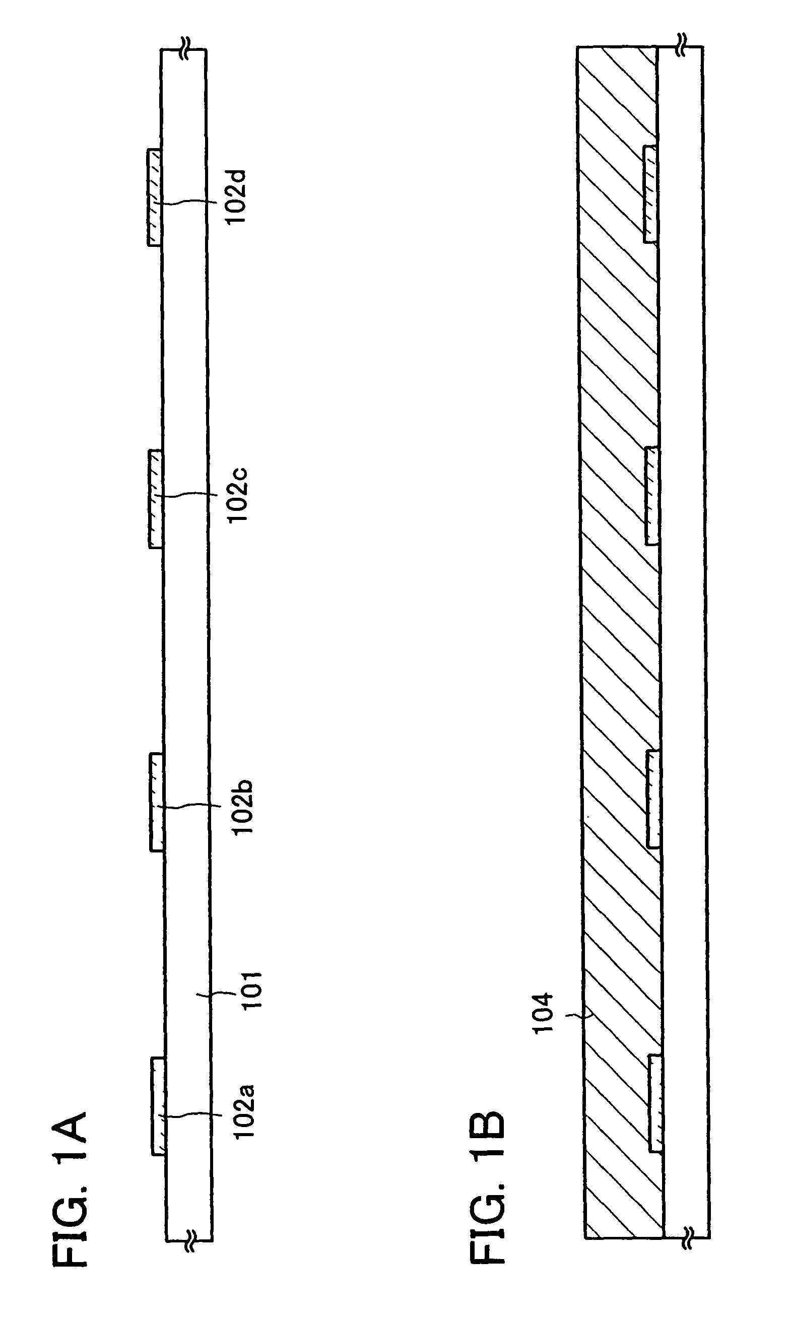
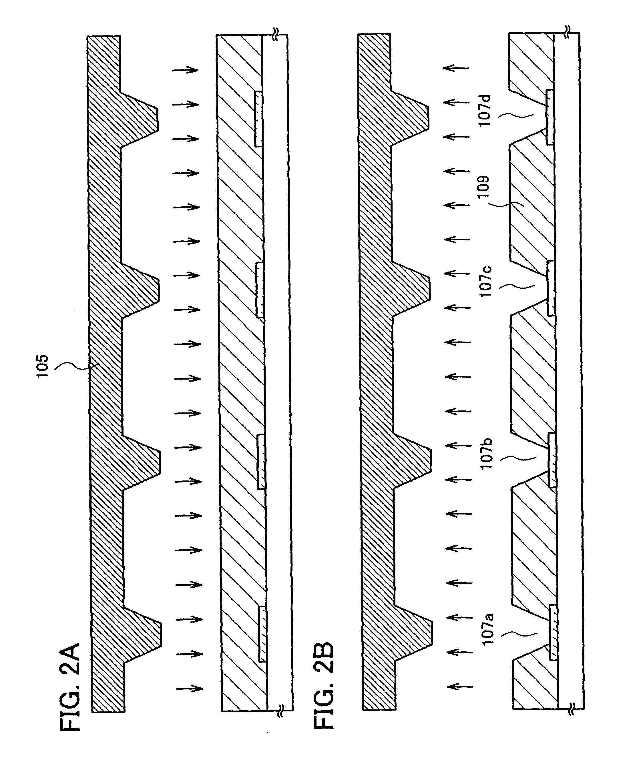
[0012]When a partition wall is formed by nano-imprinting, a partition wall which is as precise as the one formed with a stepper apparatus, that is, a partition wall with precision of nanometer (nm) can be formed. In addition, since a partition wall is formed using a mold (a casting mold) in nano-imprinting, a plurality of partition walls can be formed with excellent reproducibility, the partition wall has few variations, and manufacturing cost can be reduced.
[0018]By the present invention, a partition wall using an inorganic material can be formed by a simple method with excellent reproducibility. Accordingly, a highly durable display device in which decreasing rate of luminance is low can be manufactured.

Problems solved by technology

The method in which etching is performed using a solution containing fluorine has a defect in that a wiring is damaged due to the solution containing fluorine.
In addition, the method in which pressure is applied with a mold by an imprinting device while heating has a defect in that a silicon oxide film has to be heated to a temperature higher than a glass transition point of silicon oxide.

Method used


Image

  • Method for manufacturing semiconductor device
  • Method for manufacturing semiconductor device
  • Method for manufacturing semiconductor device

Examples


embodiment 1

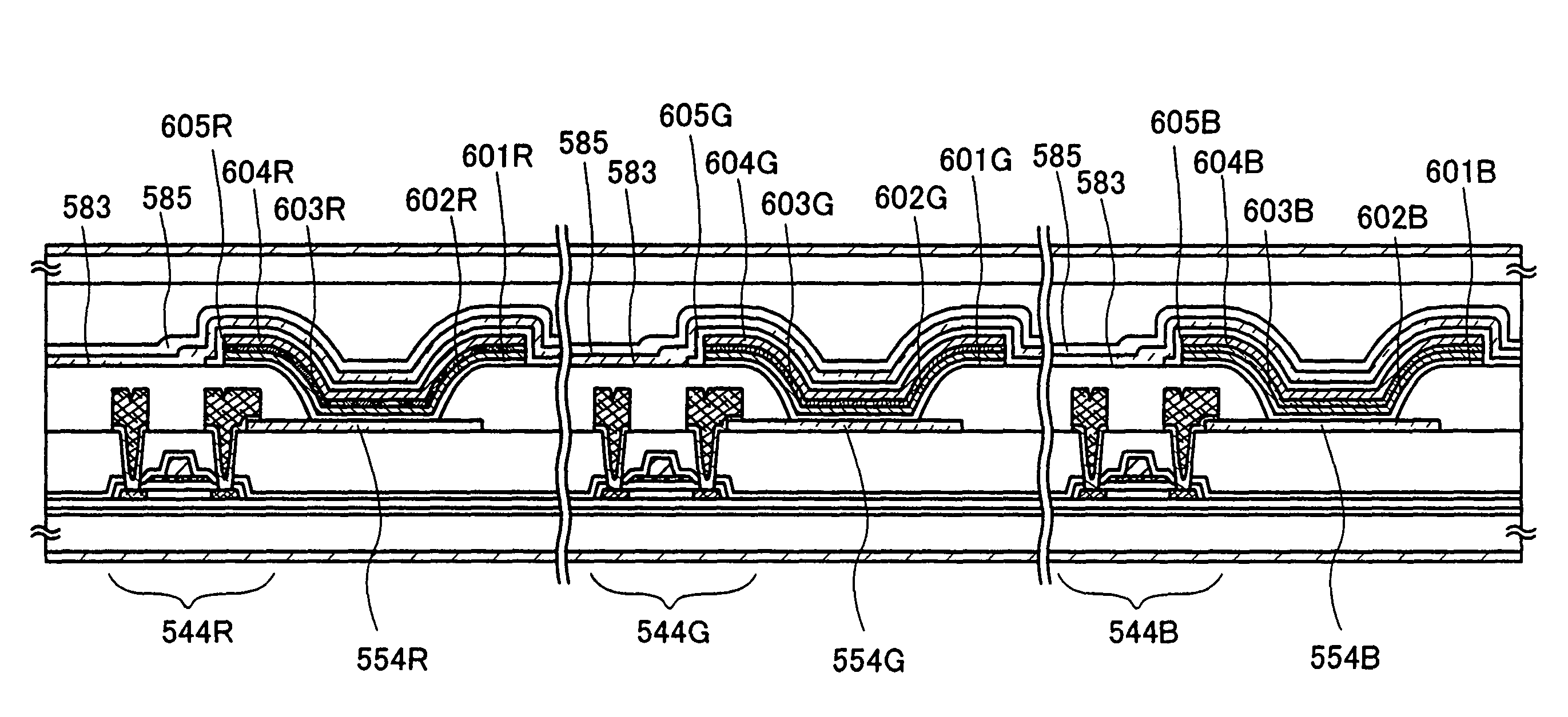
[0075]An example of using a method for manufacturing a semiconductor device of the present invention will be explained with reference to FIGS. 4A to 4D, FIGS. 5A to 5C, FIGS. 6A to 6C, FIGS. 7A and 7B, FIGS. 8A and 8B, FIGS. 9A and 9B, FIG. 10, FIG. 11, and FIG. 12.

[0076]First, as shown in FIG. 4A, a base film 502 is formed over a substrate 501. As the substrate 501, for example, a glass substrate such as barium borosilicate glass or alumino borosilicate glass, a quartz substrate, a stainless steel substrate, or the like can be used. In addition, a substrate made of plastic typified by PET (polyethylene terephthalate), PES (polyethersulfone), or PEN (polyethylene naphthalate), or a substrate made of a flexible synthetic resin such as acrylic can be used.

[0077]The base film 502 is provided in order to prevent an alkali metal such as Na or an alkaline earth metal contained in the substrate 501 from diffusing into a semiconductor film and having an adverse effect on characteristics of ...

embodiment 2

[0175]In this embodiment, an example in which the present invention is applied to an inorganic EL element will be explained with reference to FIGS. 13A to 13C and FIGS. 14A to 14C.

[0176]A light-emitting element utilizing electroluminescence is classified by whether a light-emitting material is an organic compound or an inorganic compound. In general, the former is referred to as an organic EL element and the latter is referred to as an inorganic EL element. The example in which an organic EL element is used in the present invention is described in Embodiment 1.

[0177]The inorganic EL element is classified into a dispersion type inorganic EL element and a thin film type inorganic EL element, depending on its element structure. The former and the latter are different in that the former has an electroluminescent layer in which particles of a light-emitting material are dispersed in a binder, whereas the latter has a light-emitting layer formed of a thin film of a light-emitting material...

embodiment 3

[0212]As electronic appliances to which the present invention is applied, the following can be given: a camera such as a video camera or a digital camera; a goggle type display, a navigation system; an audio reproducing device (such as a car audio component set); a computer; a game machine; a portable information terminal (such as a mobile computer, a cellular phone, a portable game machine, or an e-book reader); an image reproducing device provided with a storage medium (specifically, a device for reproducing a storage medium such as a digital versatile disc (DVD) and having a display for displaying the reproduced image), and the like.

[0213]Specific examples of the electronic appliances are shown in FIG. 15, FIG. 16, FIGS. 17A and 17B, FIG. 18, FIG. 19, FIG. 20, and FIGS. 21A to 21E.

[0214]FIG. 15 shows an EL module in which a display panel 301 and a circuit substrate 311 are combined. In the circuit substrate 311, a control circuit 312, a signal division circuit 313, and the like a...


PUM

PropertyMeasurementUnit
thicknessaaaaaaaaaa
thicknessaaaaaaaaaa
temperatureaaaaaaaaaa

Abstract

An object is to provide a semiconductor device with excellent reproducibility which is manufactured at low cost. A method for manufacturing a semiconductor device includes steps of forming a first electrode over a substrate; forming an insulating layer over the substrate and the first electrode; pressing a mold against the insulating layer to form an opening in the insulating layer; separating the mold from the insulating layer in which opening is formed; hardening the insulating layer in which the opening is formed to form a partition wall; forming a light-emitting layer over the first electrode and the partition wall; and forming a second electrode over the light-emitting layer. As a method for forming the partition wall, nano-imprinting is used. An insulating layer contains polysilane. The partition wall formed of a silicon oxide film is formed by UV light irradiation and heating.

Description

TECHNICAL FIELD[0001]The present invention relates to a semiconductor device and a method for manufacturing the same.BACKGROUND ART[0002]A plurality of pixels are formed in a display device such as an organic EL (Electro Luminescence) display, an inorganic EL display, a liquid crystal display, a plasma display, or a surface-conduction electron-emitter display (SED).[0003]A great number of resin materials are used as a material for separating a plurality of pixels (hereinafter, referred to as a partition wall) (see Patent Document 1: Japanese Published Patent Application No. 2000-294378).[0004]An organic resin (for example, polyimide or the like) is preferable as a material for a partition wall. However, an organic resin is inferior in heat resistance to many inorganic matters and has comparatively high hygroscopicity. Therefore, a small amount of moisture discharged from a partition wall by heat of a display device might cause decrease in luminance of the display device.[0005]In par...

Claims


Application Information

Patent Timeline
Patent Type & Authority Patents(United States)
IPC IPC(8): H01L51/40H01L27/32H01L29/45H01L51/56H01L27/12
CPCH01L27/3246H01L27/3283H01L29/458H01L51/56H01L27/1248H10K59/173H10K59/122H10K71/00
Inventor FUJII, TERUYUKI
Owner SEMICON ENERGY LAB CO LTD
Learn More