Perforated blocking layer for enhanced broad band response in a focal plane array

a focal plane array and blocking layer technology, applied in the field of photodetectors, can solve the problems of inability to image visible, increase power consumption, size and cost of cameras that utilize such sensors, and thermal sensing alone is not capable of imaging through common window materials. , to achieve the effect of enhancing visible response and enhancing visible respons

Active Publication Date: 2015-08-18
SENSORS UNLTD
View PDF3 Cites 19 Cited by
  • Summary
  • Abstract
  • Description
  • Claims
  • Application Information

AI Technical Summary

Benefits of technology

[0016]Advantages of at least one embodiment include enhanced visible response for SWIR imaging products. An advantage of at

Problems solved by technology

However, at least in the case of HgCdTe, because of high dark current due to the narrow bandgap, these devices must be mechanically cooled, often to cryogenic temperatures, which increases power consumption, size and cost of cameras that utilize such sensors.
Newer processes are making it possible to achieve SWIR to MWIR (1.1 μm-3.5 νm) imaging at higher operating temperatures, but SWaP (Size, Weight and Power) remain a challenge, as well, MWIR systems cannot image visible energy, such that systems requiring visible signal response (typically Blue 450 nm to red 700 nm) must also employ EO sensors for visible imaging and then merge the two datastreams with fusion algorithms or provide dual displays for managing the two separate bands.
Additionally, due to the material properties of many glasses, particularly those utilized in industrial environments, LWIR (thermal spectrum typically 8 um to 12 um) is not transmitted, but is absorbed or reflected in the medium, thus thermal sensing alone is not capable of imaging through common window materials such as in buildings or ANSI Standard protective shielding in industrial assembly l

Method used


Image

  • Perforated blocking layer for enhanced broad band response in a focal plane array
  • Perforated blocking layer for enhanced broad band response in a focal plane array
  • Perforated blocking layer for enhanced broad band response in a focal plane array

Examples


Embodiment Construction

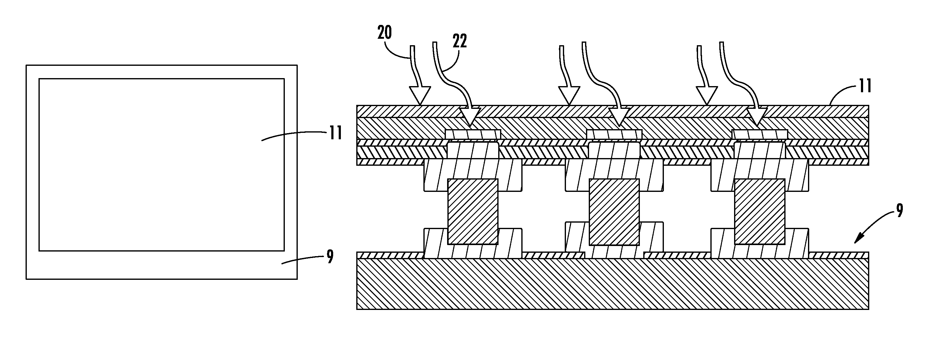
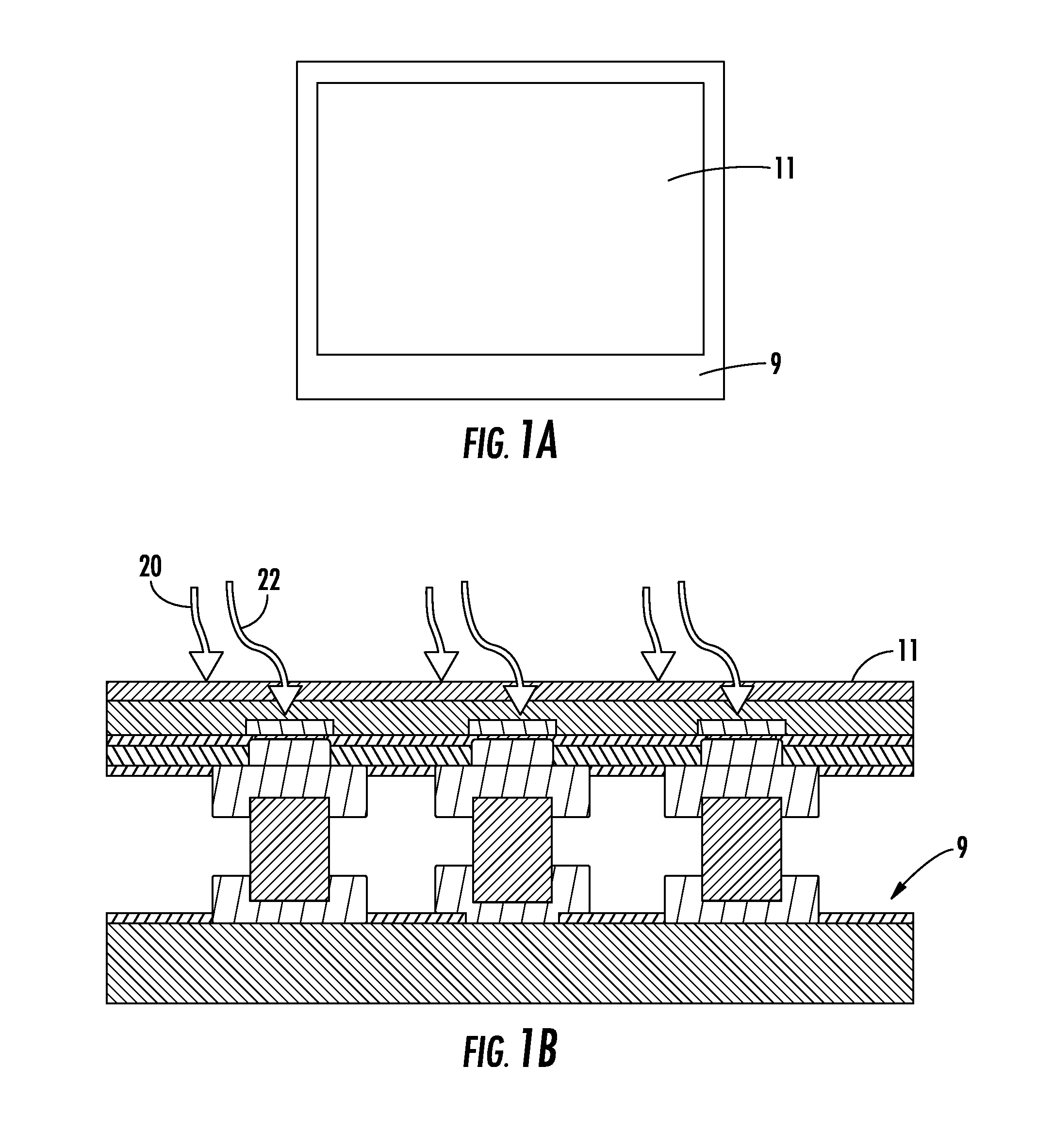
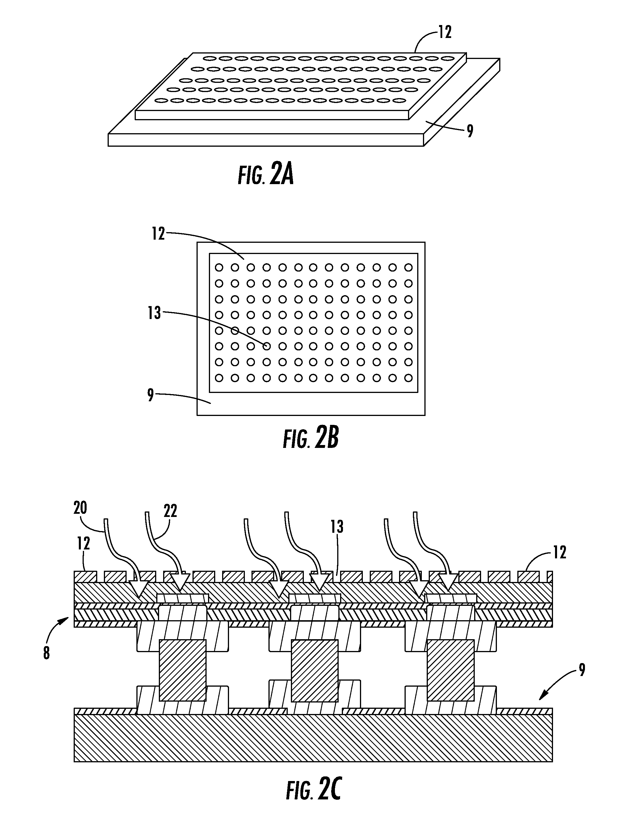
[0028]As used herein, the term “blocking layer” can refer to a surface layer, such as a back surface layer, of a photodiode which is incident to a radiation directed to the photodiode. Embodiments described herein include photodetector arrays that have been processed with a patterned etch of the substrate or remaining buffer (blocking) layer, which is the primary layer in the optical path of the incoming photon flux. Reference will now be made in detail to the present embodiments, examples of which are illustrated in the accompanying drawings. Wherever possible, the same reference numbers will be used throughout the drawings to refer to the same or like parts.

[0029]Notwithstanding that the numerical ranges and parameters setting forth the broad scope of the invention are approximations, the numerical values set forth in the specific examples are reported as precisely as possible. Any numerical value, however, inherently contains certain errors necessarily resulting from the standard...


PUM


Abstract

Provided is a focal plane array that includes an array of photodetectors, with each photodetector being in electrical communication with a corresponding one of an electrode of a read out integrated circuit. The array of photodetectors include an insulating layer, a blocking layer comprising at least one blind via, and an active layer formed between the insulating layer and the blocking layer. A first portion of the blocking layer transmits radiation having a first wavelength and reflects radiation having second wavelength that is lower than that of the first wavelength. A diameter of the at least one blind via is selected to allow radiation of the second wavelength to pass through the at least one blind via.

Description

FIELD OF THE INVENTION[0001]This invention relates generally to the field of photodetectors, particularly near-infrared (NIR) and short-wave infrared (SWIR) photodetectors, and specifically to the field of focal plane arrays comprising a plurality of photodetectors.BACKGROUND OF THE INVENTION[0002]The visible spectrum of light extends from wavelengths of about 0.4 microns to about 0.7 microns. Wavelengths longer than visible wavelengths can be detected by dedicated sensors. However, SWIR light is reflective light which bounces off of objects much like visible light. As a result of its reflective nature, detected SWIR light can have shadows and contrast in its imagery. For low light level imaging applications, noise / leakage current such as dark current must be reduced to obtain sufficient sensitivity.[0003]Sensors constructed from materials like mercury cadmium telluride (HgCdTe) or indium antimonide (InSb) can be very sensitive in the SWIR to MWIR band. However, at least in the case...

Claims


Application Information

Patent Timeline
IPC IPC(8): G01J5/20H01L27/146H01L31/18
CPCH01L27/14625H01L31/1876H01L27/14649H01L27/1465H01L27/14694H01L27/14621H01L2924/351
Inventor DIXON, PETER, E.
Owner SENSORS UNLTD
Why Eureka
Try Eureka