Flip-chip hybridization of microelectronic components by local heating of connecting elements

a technology of connecting elements and microelectronic components, applied in the field of flip-chip hybridization, can solve the problems of not being able to separate the two hybridized components, the plastic component takes a rubbery state, is even destroyed, and cannot be compatible with organic components, etc., to achieve high photonic energy input, reduce unwanted thermal effects, and reduce the effect of heat loss

Inactive Publication Date: 2015-08-18
COMMISSARIAT A LENERGIE ATOMIQUE ET AUX ENERGIES ALTERNATIVES
View PDF15 Cites 4 Cited by
  • Summary
  • Abstract
  • Description
  • Claims
  • Application Information

AI Technical Summary

Benefits of technology

[0020]More particularly, the manufacturing of the metal well comprises forming a metal area and cutting with a laser an opening in said metal area. The laser etching, for example, by means of an excimer laser, has the advantage of providing a very local heating, and thus of limiting unwanted thermal effects on the second microelectronic component, while allowing a high photonic energy input. The size of the well opening is for example adjusted by means of the difference in thermal expansion coefficients between the material of the metal area and the material of the substrate.
[0021]According to an embodiment, the electric insulator is a fluorinated polymer of low dielectric constant, particularly a dielectric constant equal or close to 2. Fluorinated polymers have a very high chemical stability, a very high melting temperature, as well as a very good thermal conductivity. Further, the insulator is advantageously obtained by applying an anneal of steep slope to an emulsion of this polymer in one or several solvents, which enables to very rapidly evaporate the solvent(s) contained in said emulsion, which generates micropores filled with air in the finally-obtained insulator.
[0022]According to an embodiment, the resistive elements are made in the form of coils or rods. Particularly, the resistive elements are series-connected. The resistive elements thus have a strong electric resistance. It is thus possible to obtain a strong heating with a low current and / or within a very short time.
[0023]According to an embodiment, on application of the current, the surface of the second microelectronic component, opposite to the surface provided with the connection elements, is cooled down, which enables to decrease the impact of the heating, even local, on the second microelectronic component.

Problems solved by technology

However, the melting of a metal bump requires high temperatures, typically higher than 156° C. Now, such temperatures are not compatible with organic components, particularly plastic components such as PEN (polyethylene naphthalate) and PET (polyethylene terephthalate), which have glass transition temperatures lower than these temperatures, respectively of 120° C. for PEN and 70° C. for PET, for example.
Thus, when submitting a plastic component to the solder bump melting temperature, the plastic component takes a rubbery state and strongly deforms, or is even destroyed.
This method is thus irreversible and does not enable to separate the two hybridized components without causing their destruction.

Method used


Image

  • Flip-chip hybridization of microelectronic components by local heating of connecting elements
  • Flip-chip hybridization of microelectronic components by local heating of connecting elements
  • Flip-chip hybridization of microelectronic components by local heating of connecting elements

Examples


first embodiment

[0049]A method for manufacturing the device just described according to the invention will now be described in further detail in relation with FIGS. 2 to 12.

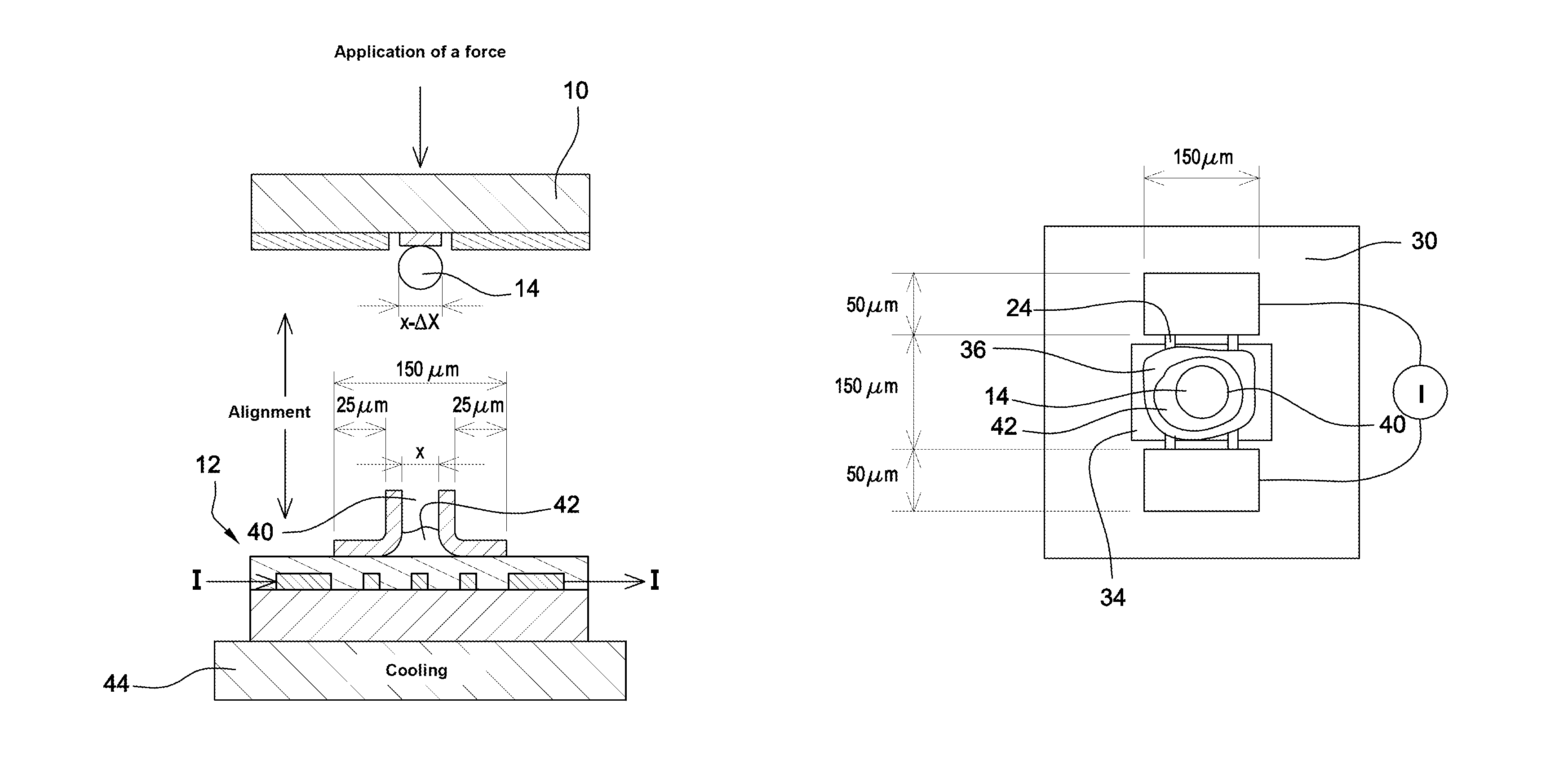
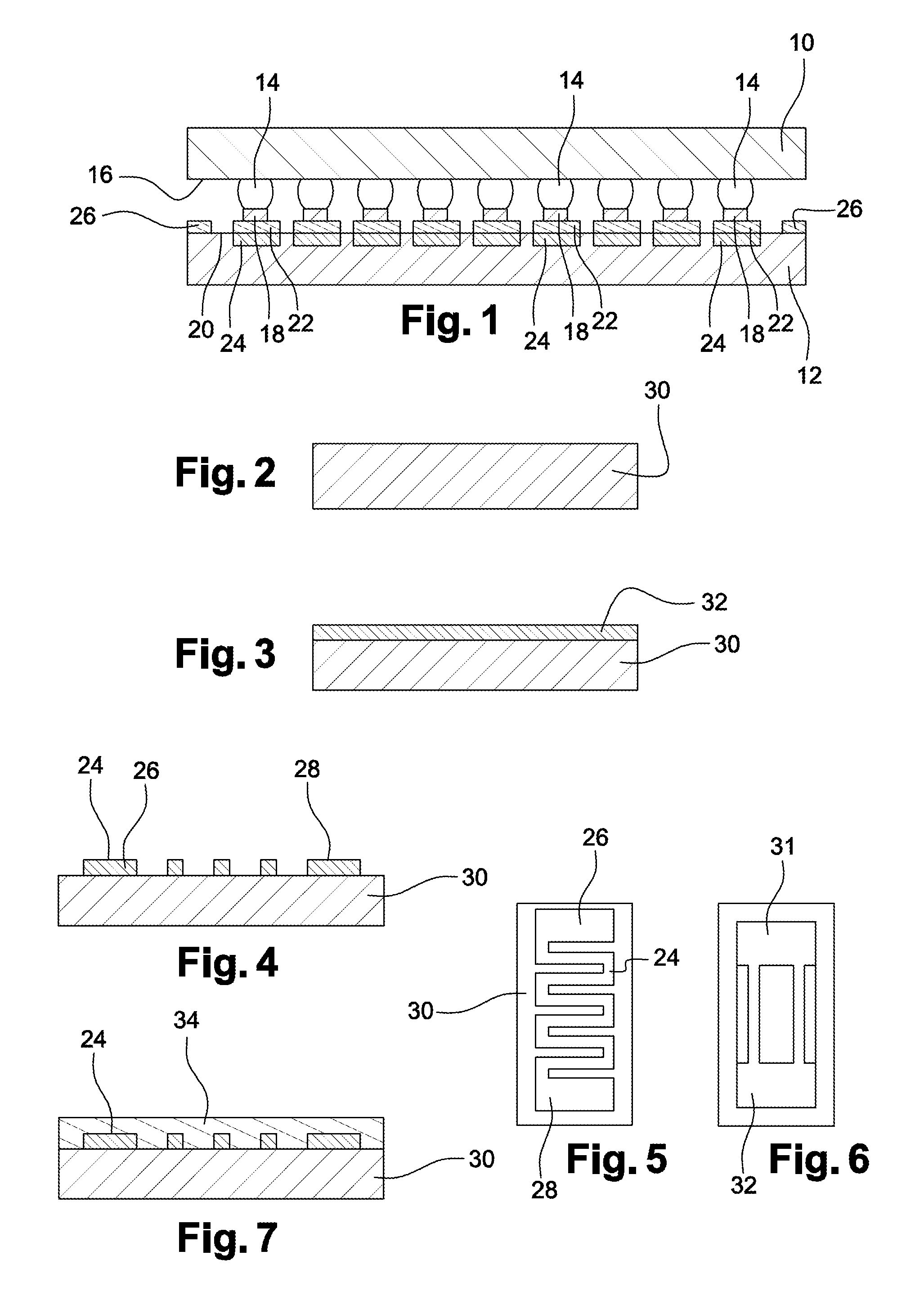
[0050]The method starts with the manufacturing of a substrate 30 of second component 12 (cross-section view of FIG. 2). Substrate 30 is for example a flexible plastic substrate particularly made of PET or of PEN, a silicon substrate comprising microelectronic circuits, or the like.

[0051]A metal layer 32 is then deposited full plate on a surface of substrate 30, for example, by evaporation or sputtering (cross-section view of FIG. 3). Layer 32 is for example a gold, titanium, nickel, copper, or tungsten layer and has a thickness in the range from 30 nanometers to 300 nanometers, to keep the flexibility of substrate 30 by limiting the effects of the difference between the thermal expansion coefficient of substrate 30 and that of metal layer 32.

[0052]Layer 32 is then etched to form resistive elements 24. The shape of elements 24 is...

second embodiment

[0067]A manufacturing method according to the invention will now be described in relation with FIGS. 13 and 14.

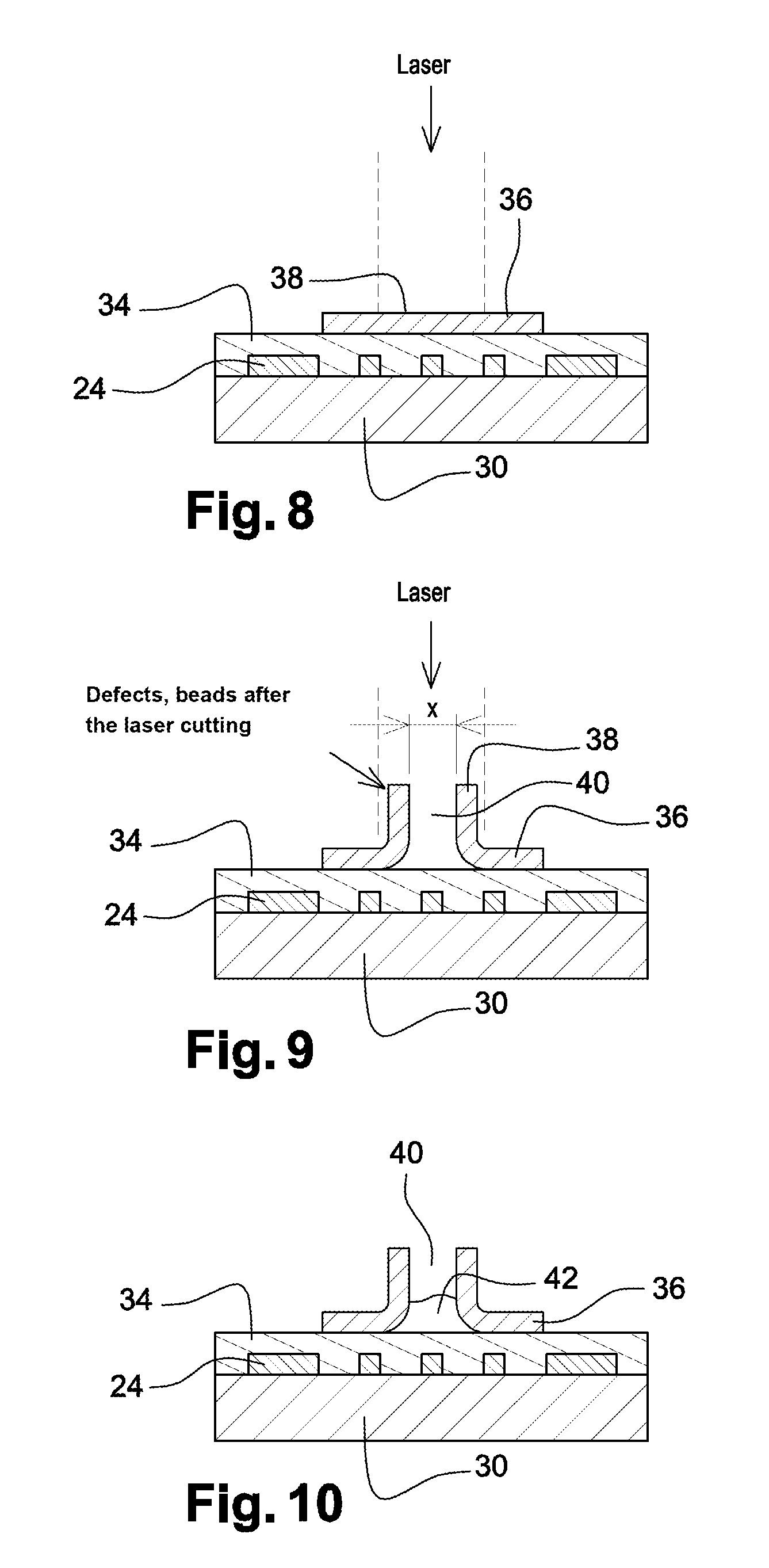
[0068]This method for example starts identically to the steps of the first embodiment described in relation with FIGS. 2 to 8. Unlike the first embodiment, the method carries on with the direct deposition of ink 42 on metal areas 36 with no forming of well 40 (cross-section view of FIG. 13). In the same way as for the first embodiment, the ink enables to use metal bumps 40 which do not or very slightly wet metal area 36, while providing an electric connection between bumps 40 and areas 36.

[0069]First component 10 is then transferred onto second component 12 by alignment of bumps 14 with areas 36 (FIG. 14). The surface of second component 12, opposite to that provided with connection elements 22 formed of areas 36 and of ink 42, is then cooled as previously described, and an electric current I is applied to each of resistive elements 24 which heat up by Joule effect. The gen...


PUM


Abstract

A method of forming a hybridized device including forming a first component provided with metal bumps, and a second component provided with connection elements, attaching the bumps to the connection elements. The manufacturing of the second component includes forming, on a surface of a substrate, resistive elements at the locations provided for the connection elements; depositing an electric insulator layer at least on the resistive elements; and forming the connection elements, each comprising a metal well having an opening capable of receiving the corresponding metal bump of the first microelectronic component and at least partially filled with a fusible element, particularly indium or an alloy of tin and gold, or with a conductive ink, particularly based on silver or copper. Further, the attachment of the balls to the connection elements comprises applying an electric current through the resistive elements to heat the bumps.

Description

FIELD OF THE INVENTION[0001]The invention relates to the assembly of microelectronic components, and more particularly to “flip-chip” hybridization.BACKGROUND[0002]An assembly by the so-called “flip-chip” technique usually comprises forming electrically-conductive bumps on a surface of a first electronic component and forming electrically-conductive connection elements, particularly bumps or connection areas, on a surface of a second component according to a predetermined connection pattern. The first component is then transferred onto the second component to place the bumps in correspondence with the connection elements, after which the assembly is pressed and heated. The bumps then deform and melt to form electric connections perpendicular to the main plane of the electronic component, generally in the form of a wafer.[0003]The most conventional technique to form the assembly is to perform a general heating of the assembly, for example, by placing the two components under a temper...

Claims


Application Information

Patent Timeline
Patent Type & Authority Patents(United States)
IPC IPC(8): H01L21/44H01L21/768H01L23/528H01L23/498H01L23/00H01L23/34
CPCH01L23/49811H01L21/76885H01L23/345H01L23/49816H01L23/49894H01L24/11H01L24/13H01L24/16H01L24/81H01L24/98H01L2224/10175H01L2224/1183H01L2224/11552H01L2224/13011H01L2224/13075H01L2224/13109H01L2224/13111H01L2224/13144H01L2224/13155H01L2224/13166H01L2224/13184H01L2224/8114H01L2224/81141H01L2224/81191H01L2224/81193H01L2224/81234H01L2224/81238H01L2224/81385H01L2224/81409H01L2224/81411H01L2224/81439H01L2224/81447H01L2224/81815H01L2924/01029H01L2924/00014H01L2924/01079H01L2924/12042H01L2924/00
Inventor ALIANE, ABDELKADER
Owner COMMISSARIAT A LENERGIE ATOMIQUE ET AUX ENERGIES ALTERNATIVES
Why Eureka
Try Eureka