

Back contact paste with Te enrichment and copper doping control in thin film photovoltaic devices
a photovoltaic device and back contact paste technology, applied in the field of back contact paste with copper doping control, can solve the problems of deterioration of graphite-paste back contacts, affecting the efficiency of solar cells, and not being generally viewed as suitable for conventional metal back contacts
Active Publication Date: 2015-10-13
FIRST SOLAR INC
View PDF26 Cites 5 Cited by
- Summary
- Abstract
- Description
- Claims
- Application Information
AI Technical Summary
Benefits of technology
The method reduces processing steps, enhances adhesion and contact between the CdTe layer and the back contact, and maintains long-term stability by consuming the acid and copper source during curing, preventing further degradation.
Problems solved by technology
Due to the high work function of CdTe, conventional metal back contacts are not generally viewed as being suitable.
However, these graphite-paste back contacts tend to degrade significantly over time, as can be shown via accelerated lifetime testing.
The degradation of the back contact electrodes undesirably leads to degradation of the solar cell efficiency, on a long-term basis.
The method involved the generation of acid by products as the paste cured and it was effective at achieving a good ohmic back contact initially, but the process was typically uncontrolled.
Method used
View moreImage
Smart ImageViewing Examples

Examples
example
[0087]An example formulation incorporating both Te enrichment and copper doping is as follows:
[0088]
SolidsComponentWeight %weight %DBE42.2—poly(vinylbutyral-co-vinylalcohol-co-vinylacetate)4.27.3art graphite42.273.0di(trimethylolpropane)tetraacrylate5.69.6bis[2-(methacryloyloxy)-ethyl]phosphate5.08.6Copper source0.10.152,2′-Azoisobutyronitrile0.81.3
[0089]Different copper sources produce different amounts of copper on the surface which is greatly dependent on the concentration of and type of acid used, the cure temperature and duration, and the size, type, and concentration of copper source used.
Login to View More PUM
| Property | Measurement | Unit |
|---|---|---|
| energy bandgap | aaaaa | aaaaa |
| thickness | aaaaa | aaaaa |
| thickness | aaaaa | aaaaa |
Abstract
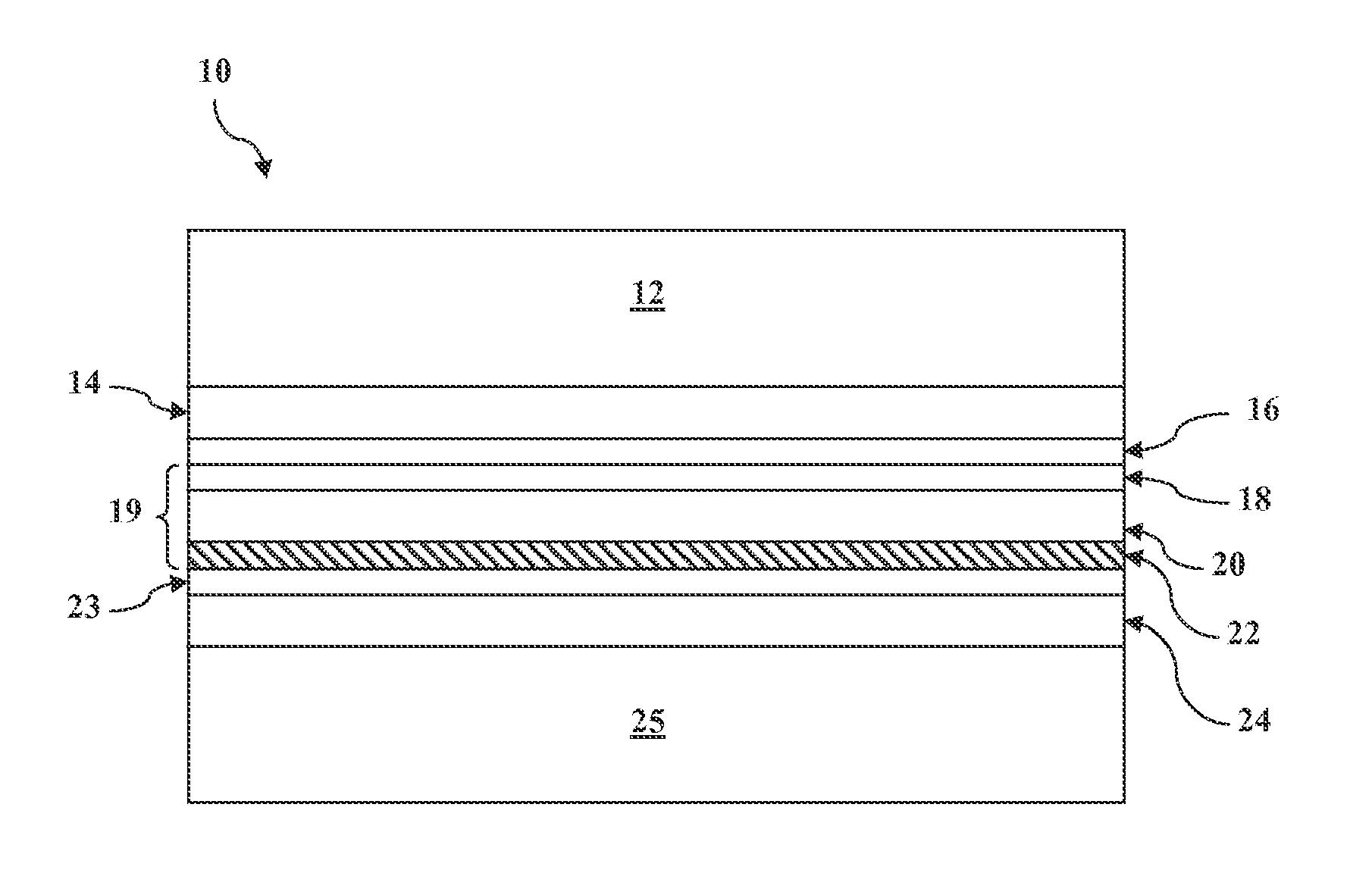
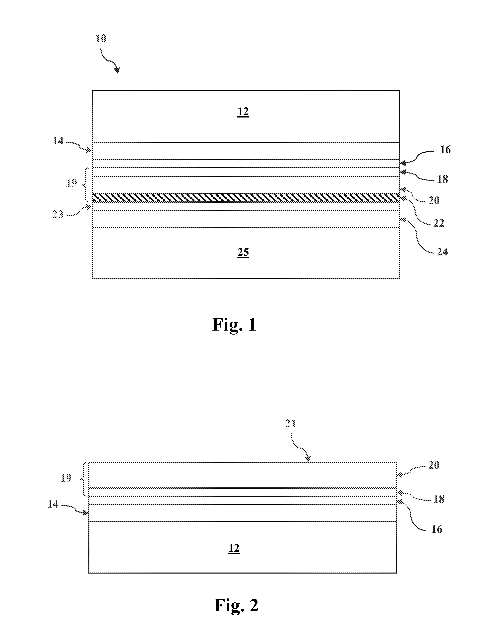
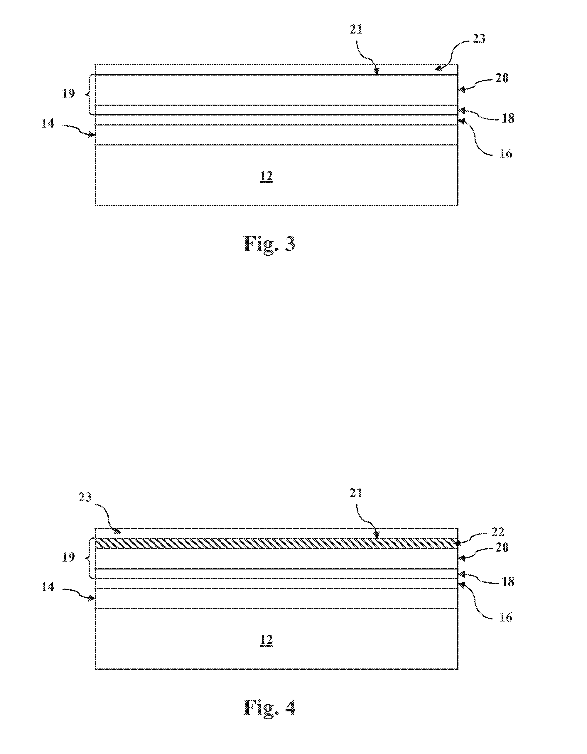
Methods for forming a back contact on a thin film photovoltaic device are provided that include applying a conductive paste onto a surface defined by a p-type absorber layer (e.g., comprising cadmium telluride) of a p-n junction and curing the conductive paste to form a conductive coating on the surface defined by a p-type absorber layer of the p-n junction. The conductive paste can include a conductive material, a solvent system, and a binder such that during curing an acid from the conductive paste reacts to enrich the surface with tellurium while copper is deposited onto the Te enriched surface. The acid is then substantially consumed during curing.
Description
FIELD OF THE INVENTION[0001]The subject matter disclosed herein relates generally to photovoltaic devices including a conductive paste as a back contact or part of a back contact of a thin film photovoltaic device.BACKGROUND OF THE INVENTION[0002]Thin film photovoltaic (PV) modules (also referred to as “solar panels”) based on cadmium telluride (CdTe) paired with cadmium sulfide (CdS) as the photo-reactive components are gaining wide acceptance and interest in the industry. CdTe is a semiconductor material having characteristics particularly suited for conversion of solar energy to electricity. For example, CdTe has an energy bandgap of about 1.45 eV, which enables it to potentially convert more energy from the solar spectrum as compared to lower bandgap semiconductor materials historically used in solar cell applications (e.g., about 1.1 eV for silicon). The junction of the n-type layer and the p-type absorber layer is generally responsible for the generation of electric potential ...
Claims
Login to View More Application Information
Patent Timeline
 Patent Type & AuthorityPatents(United States)
IPC IPC(8): H01L21/00H01L31/18H01L31/0224
CPCH01L31/022441H01L31/1828H01B1/22H01L31/022425H01L31/073H01L31/1864Y02E10/543Y02E10/547Y02P70/50
InventorLUCAS, TAMMY JANEFELDMAN-PEABODY, SCOTT DANIELCLARK, LAURA ANNECOLE, MICHAEL CHRISTOPERCORWINE, CAROLINE RAE
OwnerFIRST SOLAR INC