Organic light emitting diode

a light-emitting diode and organic technology, applied in the field of organic light-emitting diodes, can solve the problems of insufficient development of stable and efficient organic material layer materials for organic light-emitting diodes, difficult to use npb in organic light-emitting diodes requiring high current, and difficult to manufacture organic light-emitting diodes with high efficiency and a long life span. , to achieve the effect of excellent light-emi

Active Publication Date: 2016-05-03
LG CHEM LTD
View PDF39 Cites 4 Cited by
  • Summary
  • Abstract
  • Description
  • Claims
  • Application Information

AI Technical Summary

Benefits of technology

[0026]An organic light emitting diode according to the present invention comprises an exciton blocking layer comprising a compound represented by Formula 1 to confine an exciton to a light emitting layer to prevent light emitting leakage, and thus there is an effect of implementing an organic electroluminescence diode having excellent light emitting efficiency. Accordingly, it is possible to implement an organic light emitting diode having a simple and economical manufacturing process, a low voltage, high efficiency, and a long life span as compared to the related art.

Problems solved by technology

Recently, NPB, which has mostly been used as the hole transport layer material, has a glass transition temperature of 100° C. or lower, and thus there is a problem in that it is difficult to use NPB in an organic light emitting diode requiring high current.
In the case of PEDOT:PSS currently used as a hole transport material in an organic light emitting diode manufactured by a solution coating method, since a LUMO energy level thereof is lower than that of an organic material used as a light emitting layer material, it is difficult to manufacture an organic light emitting diode having high efficiency and a long life span.
In order to sufficiently exhibit excellent characteristics of the aforementioned organic light emitting diode, a material forming the organic material layer in the diode, for example, the hole injection material, the hole transport material, the light emitting material, the electron transport material, the electron injection material, and the like should be supported by stable and efficient materials in advance, but development of a stable and efficient organic material layer material for organic light emitting diodes has not yet been sufficiently made, such that there is still a demand for developing a new material.

Method used


Image

  • Organic light emitting diode
  • Organic light emitting diode
  • Organic light emitting diode

Examples


example

Example 1

Manufacturing of the Organic Light Emitting Diode

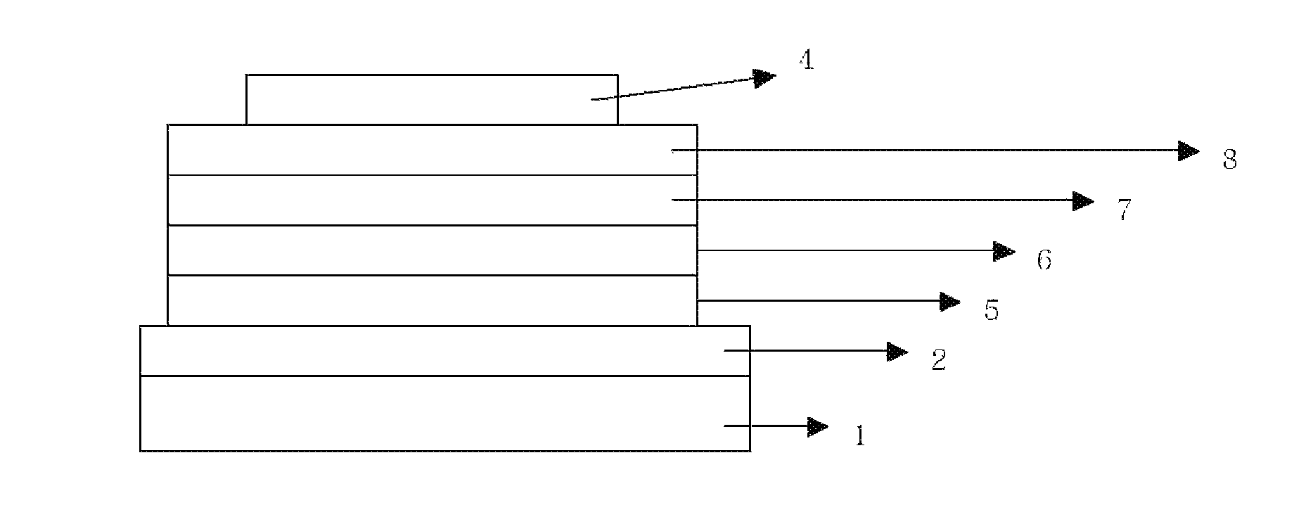
[0075]The glass substrate (corning 7059 glass) on which the thin film of ITO (indium tin oxide) was applied to a thickness of 1,000 Å was immersed in distilled water having the detergent dissolved therein, and washed by the ultrasonic wave. In this case, the detergent as used herein was the product commercially available from Fischer Co. and the distilled water was one which had been twice filtered by using the filter commercially available from Millipore Co. ITO was washed for 30 mins, and washing with ultrasonic waves was then repeated twice for 10 mins by using distilled water. After the completion of washing with distilled water, washing with ultrasonic waves was performed by using solvents such as isopropyl alcohol, acetone, and methanol, and the resulting product was dried and transported to the plasma washing machine. Further, the substrate was dry-washed by using the oxygen plasma for 5 mins, and then transported to t...

example 2

Manufacturing of the Organic Light Emitting Diode

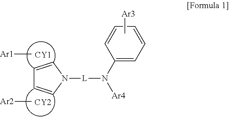
[0079]The same diode was manufactured, except that the compound of Formula EB-4 used as the electron blocking layer in Example 1 was substituted by the compound of the following Formula EB-5.

[0080]

example 3

Manufacturing of the Organic Light Emitting Diode

[0081]The same diode was manufactured, except that the compound of Formula EB-4 used as the electron blocking layer in Example 1 was substituted by the compound of the following Formula EB-6.

[0082]


PUM

PropertyMeasurementUnit
glass transition temperatureaaaaaaaaaa
thicknessaaaaaaaaaa
thicknessaaaaaaaaaa

Abstract

The present invention relates to an organic light emitting diode and a method of manufacturing the same. An organic light emitting diode according to the present invention comprises an exciton blocking layer comprising a compound represented by Formula 1 to confine an exciton to a light emitting layer to prevent light emitting leakage, and thus there is an effect of implementing an organic electroluminescence diode having excellent light emitting efficiency. Accordingly, it is possible to implement an organic light emitting diode having a simple and economical manufacturing process, a low voltage, high efficiency, and a long life span as compared to the related art.

Description

[0001]This application is a 35 USC §371 National Stage entry of International Application No. PCT / KR2013 / 001577, filed on Feb. 27, 2013, which claims priority of Korean Application No. 10-2012-0019965, filed on Feb. 27, 2012, all of which are hereby incorporated by reference in their entirety.TECHNICAL FIELD[0002]The present invention relates to an organic light emitting diode. More particularly, the present invention relates to an organic light emitting diode having excellent characteristics comprising a low voltage, high efficiency, and a long life span, and a simple manufacturing process.BACKGROUND ART[0003]An organic light emitting phenomenon is an example of a conversion of current into visible rays by an internal process of a specific organic molecule. The organic light emitting phenomenon is based on the following principle. When an organic material layer is interposed between an anode and a cathode, if voltage is applied between two electrodes, electrons and holes are inject...

Claims


Application Information

Patent Timeline
Patent Type & Authority Patents(United States)
IPC IPC(8): H01L51/50H05B33/20H01L51/00H01L51/54C09K11/06
CPCH01L51/006H01L51/0052H01L51/0054H01L51/0058H01L51/0061H01L51/0067H01L51/0068H01L51/0072H01L51/0073H01L51/0074H01L51/50H05B33/20C09K11/06H01L51/5056H01L51/5096H10K85/622H10K85/655H10K85/636H10K85/626H10K85/633H10K85/654H10K85/6576H10K85/6574H10K85/6572H10K50/18H10K50/15H10K85/615H10K50/11H10K50/00
Inventor HONG, SUNG KILCHUN, MINSEUNGKIM, KONGKYEOMJANG, JUNGIKIM, YUN HWANLEE, DONG HOON
Owner LG CHEM LTD
Why Eureka
Try Eureka