Method and apparatus for single chamber treatment

a single chamber treatment and apparatus technology, applied in the direction of semiconductor/solid-state device details, coatings, transistors, etc., can solve the problems of increasing severe problems, unsatisfactory thermal cycling and stress migration resistance in interconnect structures, etc., to enhance interfacial adhesion, enhance diffusion barrier properties, and enhance ald/cvd deposition

Inactive Publication Date: 2017-07-11
ELPIS TECH INC
View PDF10 Cites 0 Cited by
  • Summary
  • Abstract
  • Description
  • Claims
  • Application Information

AI Technical Summary

Benefits of technology

[0007]In one embodiment, the disclosure relates to a method, system and apparatus for single chamber treatment of a semiconductor device. In one embodiment, the single chamber may be used for dielectric surface modification and selective compound removal. An exemplary dielectric surface modification may modify one or more surface properties of the semiconductor device being constructed. For example, the surface properties may be modified from hydrophobic to hydrophilic, densify the dielectric layer and / or increase copper (Cu) diffusion barrier properties. The modified dielectric surface enables advanced thin film depositions (i.e., enhanced nucleation of ALD / CVD deposition as well as enhanced interfacial adhesion.

Problems solved by technology

The major problem encountered in this area today is poor mechanical integrity of deep submicron metal studs embedded in low k dielectric materials, which can cause unsatisfied thermal cycling and stress migration resistance in interconnect structures.
This problem becomes increasingly severe when either new metallization approaches or porous low k dielectric materials are used.

Method used


Image

  • Method and apparatus for single chamber treatment
  • Method and apparatus for single chamber treatment
  • Method and apparatus for single chamber treatment

Examples


Embodiment Construction

[0013]In on embodiment, the disclosure relates to microchip processing that in a single chamber and at a single processing unit. The processing may include modifying the dielectric surface condition and selective removal of metal compounds from the microchip surface. Conventional methods implemented these steps in two different chambers which is time consuming, error prone and expensive. In one embodiment, the dielectric surface modification can result in changing the microchip surface from a hydrophobic to hydrophilic surface. The surface density may also be increased in this process. The surface compound may include Silicon (Si), Nitrogen (N2), Ammonia (NH3), Phosphorous (P), Boron (B), Oxygen (O2) or other chemicals. Two process conditions may be included: thermal and direct plasma.

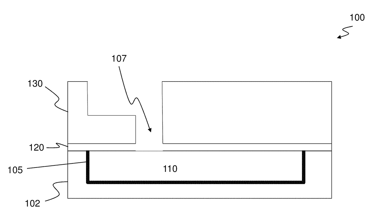
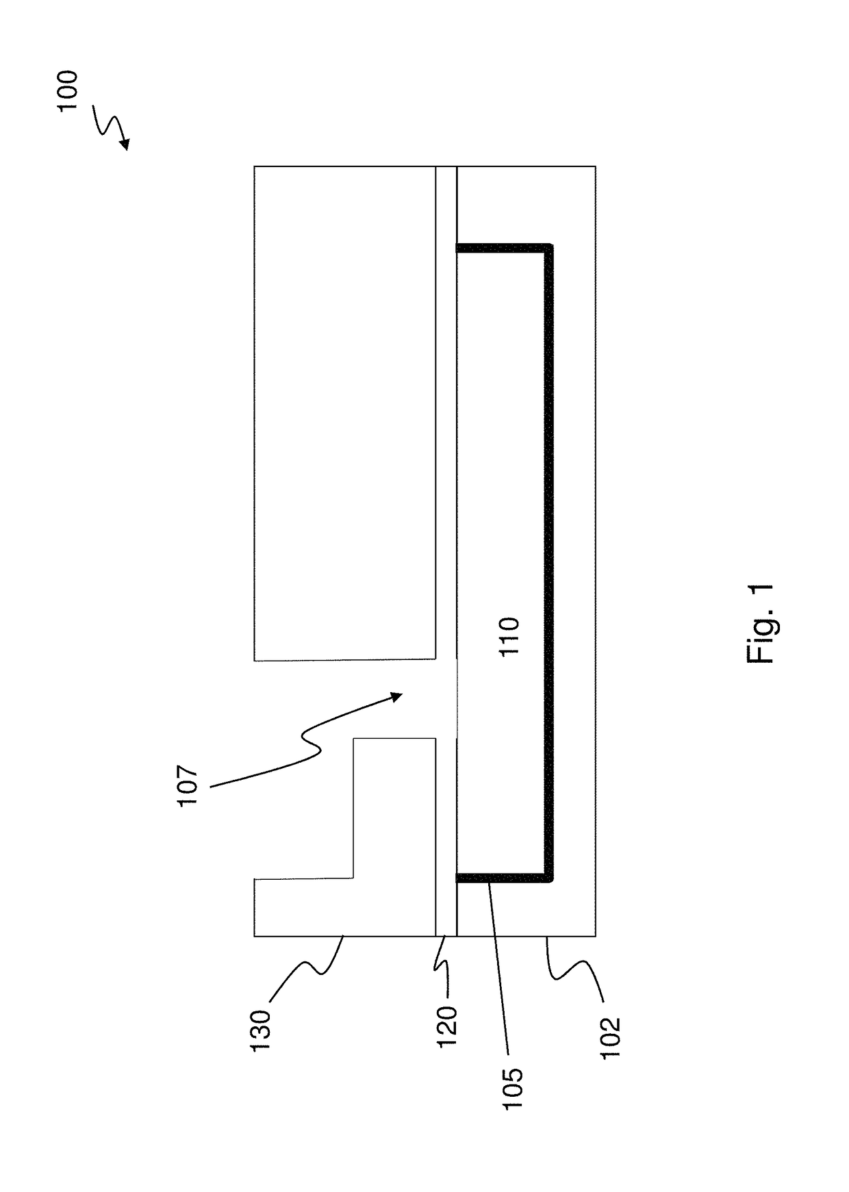
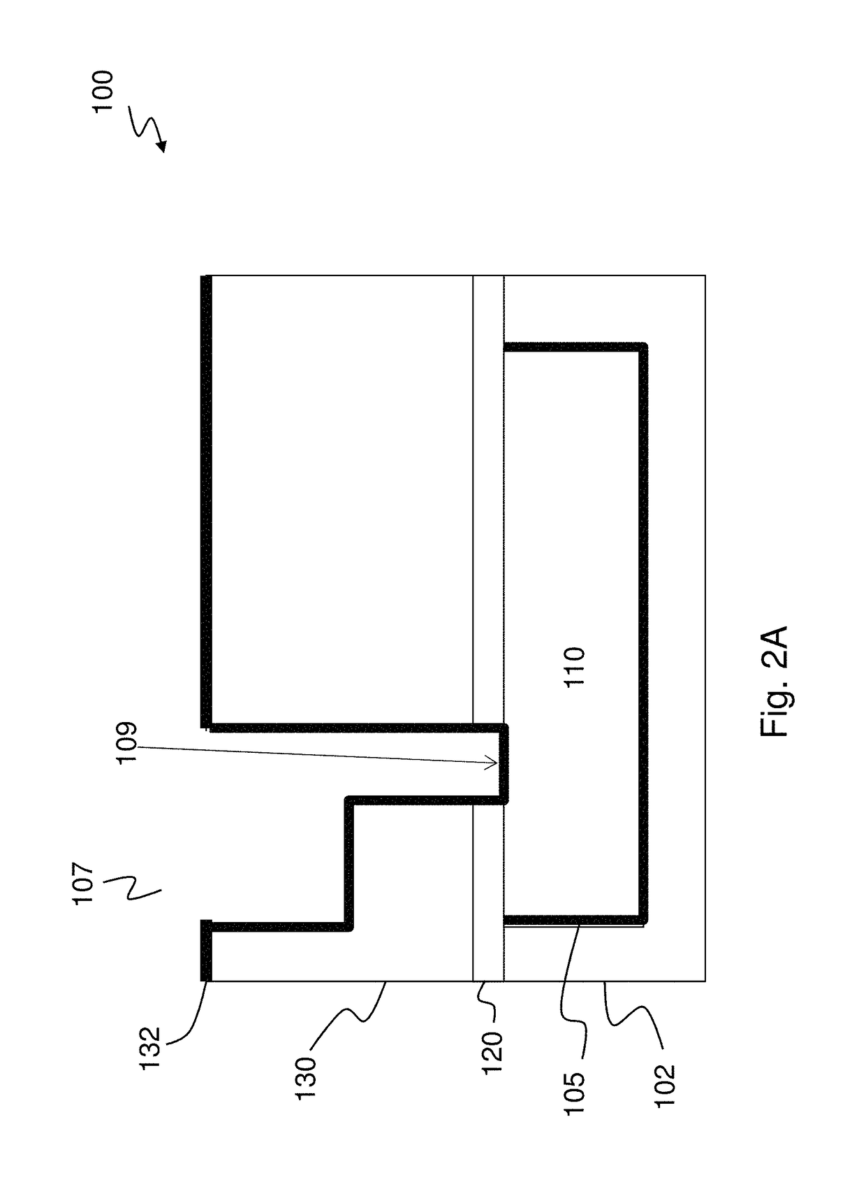
[0014]FIG. 1 schematically shows post dielectric patterning of a microchip according to one embodiment of the disclosure. Microchip 100 of FIG. 1 includes insulator layer 102, conductor layer 110, capp...


PUM

PropertyMeasurementUnit
electrical biasaaaaaaaaaa
hydrophobicaaaaaaaaaa
hydrophilicaaaaaaaaaa

Abstract

The disclosure relates to using a single chamber for multiple treatments resulting in a semiconductor chip having an interconnect. An exemplary process many include forming a via to expose several layers of a microchip. The layers may include, pattered dielectric layer, a capping layer, a first metal layer and an insulator. A surface modification step is then implemented to modify and / or densify the treated surfaces of the dielectric surface. A metal compound removal step is then implemented to remove metal compounds from the bottom of the via. Finally, the via is filled with a conductive material. The surface modification and the metal compound removal steps are implemented in one chamber.

Description

[0001]This application is a continuation of application Ser. No. 15 / 130,814, filed Apr. 15, 2016, and claims the filing date priority thereof. The disclosure of application Ser. No. 15 / 130,814 is incorporated herein in its entirety.BACKGROUND[0002]Field[0003]The disclosure relates to a method, apparatus and system to provide single chamber treatment for dielectric surface modification and selective metal compound removal[0004]Description of Related Art[0005]Conventional semiconductor devices include a plurality of circuits which form an integrated circuit fabricated on a semiconductor substrate. A complex network of signal paths will normally be routed to connect the circuit elements distributed on the surface of the substrate. Efficient routing of these signals across the device requires formation of multilevel or multilayered schemes, such as, for example, single or dual damascene wiring structures. Within a typical interconnect structure, metal vias run perpendicular to the semic...

Claims


Application Information

Patent Timeline
Patent Type & Authority Patents(United States)
IPC IPC(8): H01L21/768C23C16/455C23C16/50H01L27/108H01L21/67
CPCC23C16/45544C23C16/50H01L21/76841H01L27/1087H01L21/67098H01L21/76843H01L21/76883H01L21/76885H01L21/7684H01L21/76814H01L21/76826H01L21/76831H01L21/76834H01L23/522H10B12/0387H01L21/3212H01L21/76802H01L21/76861H01L23/5226H01L23/528H01L23/53238
Inventor YANG, CHIH-CHAOEDELSTEIN, DANIEL CHARLES
Owner ELPIS TECH INC
Why Eureka
Try Eureka