Transparent conductive film and electro-optical device having the same

a technology of transparent conductive film and electro-optical device, which is applied in the direction of organic semiconductor device, sustainable manufacturing/processing, final product manufacturing, etc., can solve the problems of high manufacturing cost, and high sheet resistance of traditional ito transparent conductive substrate. , to achieve the effect of high sheet resistance, high manufacturing cost and poor flexibility

Active Publication Date: 2018-01-16
NATIONAL TSING HUA UNIVERSITY
View PDF4 Cites 3 Cited by
  • Summary
  • Abstract
  • Description
  • Claims
  • Application Information

AI Technical Summary

Benefits of technology

[0011]The primary objective of the present invention is to provide a transparent conductive film and electro-optical devices having the same. Compared to traditional ITO transparent substrate showing drawbacks of high sheet resistance, poor flexibility and high manufacturing cost, the present invention mainly discloses a transparent conductive film fabricated by sequentially forming a wetting layer and an ultra-thin metal layer onto a transparent substrate, ...

Problems solved by technology

However, with the growing of demands made by market on All-in-One PCs, large-scale notebooks and displays with large-size touch panel, expensive manufacturing cost and high sheet resistance of traditional ITO transparent conductive substrate have become the major problems of the large-size touch panel.
Literature 1 has reported that the light emission performance of the typical OLED 1′ is limited due to low out-coupling efficiency.
Moreover, light path C′ is called substrate influence to the emission light, which means a significant portion of the generated light is confined within the glass-ITO interface due to interference effec...

Method used


Image

  • Transparent conductive film and electro-optical device having the same
  • Transparent conductive film and electro-optical device having the same
  • Transparent conductive film and electro-optical device having the same

Examples


first application embodiment

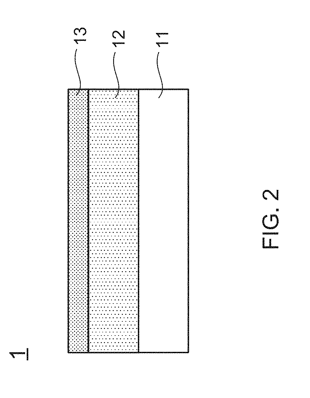
[0065 of the Transparent Conductive Film

[0066]Above descriptions have clearly introduced the constitution, features and advantages of the transparent conductive film of the present invention. Subsequently, some electro-optical devices having the transparent conductive film will be introduced in following paragraphs. Please refer to FIG. 7, which illustrates a schematic cross-sectional side view of an organic light-emitting diode (OLED) having the transparent conductive film of the present invention. As FIG. 7 shows, the OLED 2 mainly comprises: the transparent conductive film 1 of the present invention, an organic active layer 21 and a cathode layer 22.

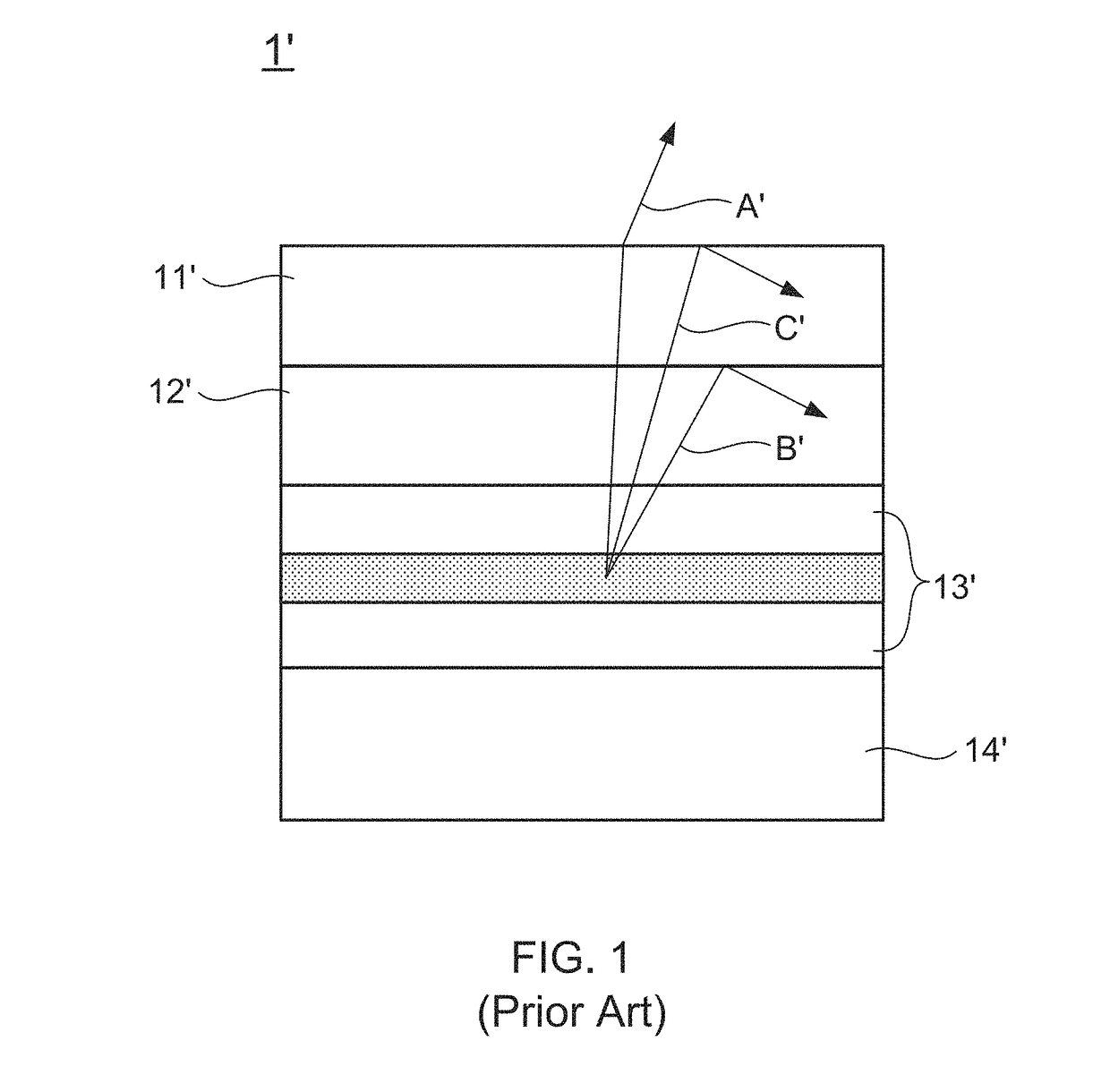
[0067]It is worth noting that, the transparent conductive film 1 further comprises an anti-reflective layer 14 disposed between the organic active layer 21 and the metal layer 13, so as to facilitate the OLED 2 exhibit outstanding performance on its out-coupling efficiency (ηout), external quantum efficiency (EQE) and power efficiency...

second application embodiment

[0082 of the Transparent Conductive Film

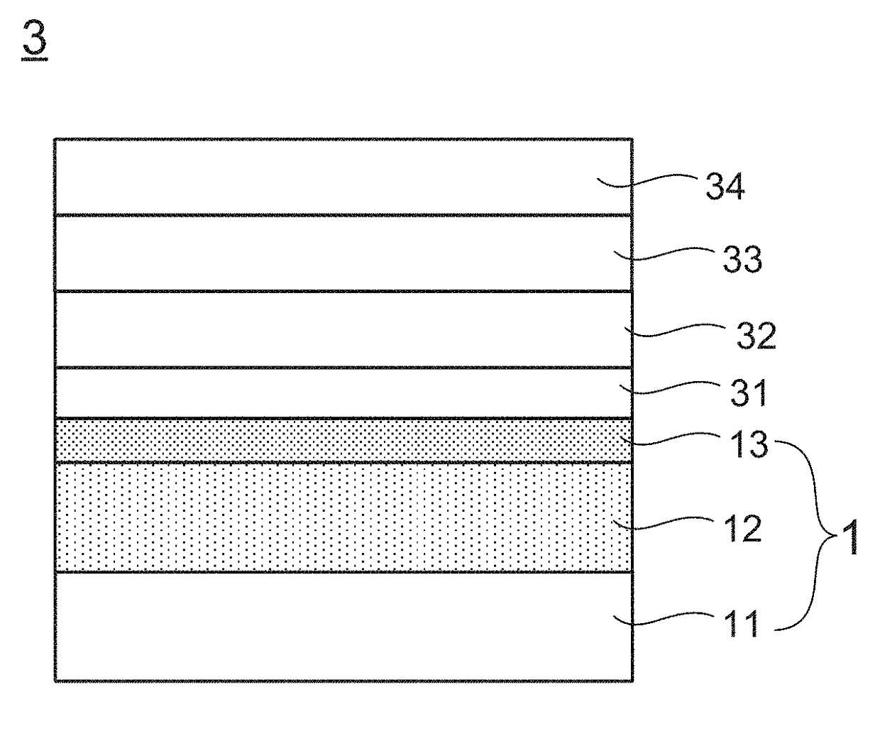
[0083]The transparent conductive film 1 of the present invention can also be applied in the fabrication of conventional organic solar cells. Please refer to FIG. 12, which illustrates a schematic cross-sectional side view of an organic solar cell having the transparent conductive film of the present invention. As FIG. 12 shows, the organic solar cell 3 comprises: the transparent conductive film 1 of the present invention, an electron extraction layer 31, a photoactive layer 32, a hole transport layer 33, and an electrode layer 34, wherein the electron extraction layer 31 is also called electron transport layer.

[0084]As engineers skilled in the development and manufacture of organic solar cells know, the photoactive layer 32 comprises a donor material and an acceptor material. In the second application embodiment, the donor material is PTB7 (Poly[[4,8-bis[(2-ethylhexyl)oxy]benzo[1,2-b′]dithiophene-2,6-diyl][3-fluoro-2-[(2-ethylhexyl)carbonyl]th...


PUM

PropertyMeasurementUnit
Thicknessaaaaaaaaaa
Thicknessaaaaaaaaaa
Thicknessaaaaaaaaaa

Abstract

Compared to traditional ITO transparent substrate showing drawbacks of high sheet resistance, poor flexibility and high manufacturing cost, the present invention mainly discloses a transparent conductive film fabricated by sequentially forming a wetting layer and an ultra-thin metal layer onto a transparent substrate, wherein the transparent conductive film includes advantages of low sheet resistance, high transmittance, great flexibility, and low manufacturing cost. Moreover, a variety of experiment data have proved that, this novel transparent conductive film can not only be applied in the fabrication of some electro-optical devices such as organic solar cell and OLED, but also helpful to the enhancement of the fundamental and essential characteristics of the electro-optical devices.

Description

BACKGROUND OF THE INVENTION1. Field of the Invention[0001]The present invention relates to the technology field of ultra-thin and highly-conductive metal electrodes, and more particularly to a transparent conductive film and electro-optical devices having the same.2. Description of the Prior Art[0002]It is well known that touch panels comprising transparent conductive substrate and sensing circuitry are mainly applied in the electronic devices with small screen size such as smart phone and tablet PC. However, with the growing of demands made by market on All-in-One PCs, large-scale notebooks and displays with large-size touch panel, expensive manufacturing cost and high sheet resistance of traditional ITO transparent conductive substrate have become the major problems of the large-size touch panel. As the person skilled in development and manufacture of the transparent conductive substrates knows, the cost of forming ITO electrode layer occupies forty percent of a total manufacturin...

Claims


Application Information

Patent Timeline
IPC IPC(8): H01L51/00H01L51/44H01L51/50H01L51/52
CPCH01L51/442H01L51/5056H01L51/5281H01L51/5234H01L51/0072H01L2251/301H01L2251/558H01L51/0037H01L51/0035H01L51/005H01L51/0078H01L51/0056H01L51/0047H01L51/0053Y02E10/549Y02P70/50H10K30/82H10K50/15H10K50/86H10K50/828H10K85/60H10K85/111H10K85/215H10K85/311H10K85/621H10K85/624H10K85/1135H10K85/6572H10K2102/00H10K2102/351
Inventor LIN, HAO-WUSHIAU, YU-CHENG
Owner NATIONAL TSING HUA UNIVERSITY
Why Eureka
Try Eureka