
Method for structuring field effect transistor in multiple channels from Nano carbon tubes

A technology of field-effect transistors and carbon nanotubes, applied in semiconductor/solid-state device manufacturing, electrical components, circuits, etc., can solve problems affecting transistor performance, large source-drain electrode size, and inability to form ohmic contacts, etc., to achieve good structural stability performance, the effect of good switching performance

Inactive Publication Date: 2008-02-06
SHANGHAI JIAO TONG UNIV
View PDF4 Cites 0 Cited by
  • Summary
  • Abstract
  • Description
  • Claims
  • Application Information

AI Technical Summary

Problems solved by technology

Its shortcoming is: the carbon nanotubes in the arrayed carbon nanotube film that this method makes piles up together, can't effectively evenly disperse, and this will make carbon nanotubes and source-drain electrode can't form good ohmic contact, carbon nanotubes There is a coupling effect between them, which affects the performance of the transistor
Moreover, the size of the source and drain electrodes used in the fabrication of arrayed carbon nanotube thin film transistors by this method is very large, with a pitch of 0.1-0.5 millimeters and a width of 50-66 millimeters, while the size of transistors in integrated circuits is much smaller than this, so this method does not Suitable for the fabrication of integrated circuit field effect transistors

Method used


Image

  • Method for structuring field effect transistor in multiple channels from Nano carbon tubes
  • Method for structuring field effect transistor in multiple channels from Nano carbon tubes

Examples


Embodiment 1

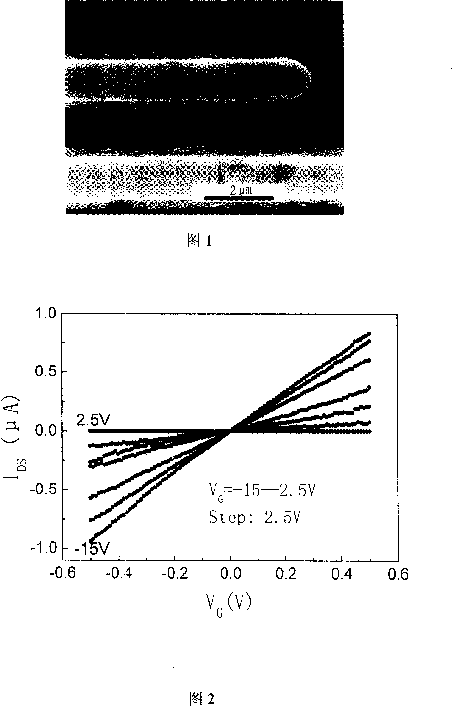
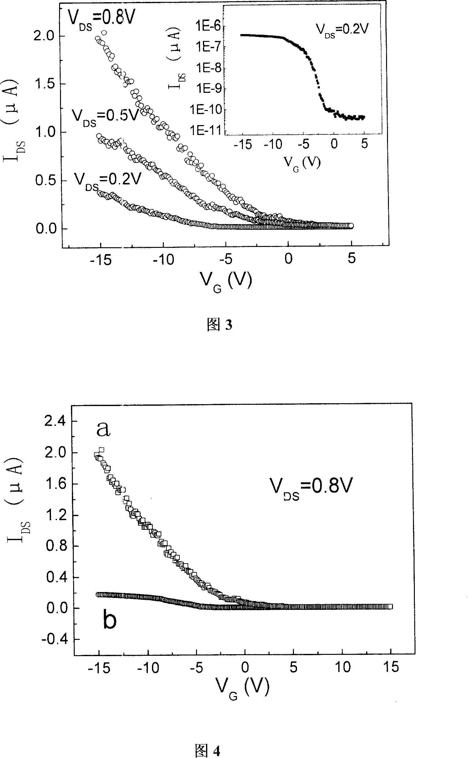
[0031] In this embodiment, a multi-channel field-effect transistor is prepared by directional arrangement of carbon nanotubes chemically modified by surface functional molecules in an alternating electric field. Firstly, the carbon nanotubes are subjected to surface activation treatment, and the carbon nanotubes are refluxed at 100° C. for 30 minutes in a mixed acid prepared by a ratio of 3:1 of concentrated sulfuric acid (concentration: 98%) and concentrated nitric acid (concentration: 68%). Active carboxyl groups are generated on the surface of carbon nanotubes to facilitate the grafting of octadecylamine or DNA molecules on the surface of carbon nanotubes. The carbon nanotubes after the surface activation treatment were reacted with octadecylamine and N, N'-dicyclohexylcarbodiimide (DCC) in a ratio of 1:100:30 (mass ratio), at 60°C React for 24 hours to graft octadecylamine on the surface of carbon nanotubes; use a filter membrane with a pore size of 2 μm for suction filtra...

Embodiment 2

[0035] In this embodiment, a multi-channel field-effect transistor is prepared by directional arrangement of carbon nanotubes chemically modified by surface functional molecules in an alternating electric field. Firstly, the carbon nanotubes are subjected to surface activation treatment, and the carbon nanotubes are refluxed at 140° C. for 30 minutes in a mixed acid prepared by a ratio of 3:1 of concentrated sulfuric acid (concentration: 98%) and concentrated nitric acid (concentration: 68%). Active carboxyl groups are generated on the surface of carbon nanotubes to facilitate the grafting of octadecylamine or DNA molecules on the surface of carbon nanotubes. The carbon nanotubes after the surface activation treatment were reacted with octadecylamine and N, N'-dicyclohexylcarbodiimide (DCC) in a ratio of 1:100:30 (mass ratio), at 110°C React for 24 hours to graft octadecylamine on the surface of carbon nanotubes; use a filter membrane with a pore size of 2 μm for suction filtr...

Embodiment 3

[0038] In this embodiment, a multi-channel field-effect transistor is prepared by directional arrangement of carbon nanotubes chemically modified by surface functional molecules in an alternating electric field. Firstly, the carbon nanotubes are subjected to surface activation treatment, and the carbon nanotubes are refluxed at 120° C. for 30 minutes in a mixed acid prepared by a ratio of 3:1 of concentrated sulfuric acid (concentration: 98%) and concentrated nitric acid (concentration: 68%). Active carboxyl groups are generated on the surface of carbon nanotubes to facilitate the grafting of octadecylamine or DNA molecules on the surface of carbon nanotubes. The carbon nanotubes after the surface activation treatment were reacted with octadecylamine and N,N'-dicyclohexylcarbodiimide (DCC) in a ratio of 1:100:30 (mass ratio), at 90°C React for 24 hours to graft octadecylamine on the surface of carbon nanotubes; use a filter membrane with a pore size of 2 μm for suction filtrat...


PUM

PropertyMeasurementUnit
strengthaaaaaaaaaa
wavelengthaaaaaaaaaa

Abstract

The method includes following steps: (1) carrying out surface activation treatment for Nano carbon tube; (2) carrying out chemical modification or DNA modification of surface functional molecule for Nano carbon tube in order to prepare stable and dispersive suspension liquid of Nano carbon tube; (3) fabricating pattern of electrode couple on surface of silicon piece of containing insulating layer through photo etching; (4) dripping suspension liquid of Nano carbon tube onto surface of electrode couple prepared in step (3) to form even distributed liquid layer; (5) applying DC or AC electric field to implement multiple strips of Nano carbon tube to let them connect to between two kinds of electrodes dividually and in parallel; (6) carrying out irradiation treatment for device of field effect transistor (FET) prepared at step (5) through ultraviolet radiation. The invention can control multiple strips of Nano carbon tube to construct channels for FET or to be as leads for electrodes.

Description

technical field [0001] The invention relates to a method for preparing a field effect transistor used in the technical field of electronic device manufacturing, specifically, a method for manufacturing a multi-channel field effect transistor whose channel is formed of carbon nanotubes. Background technique [0002] At present, the preparation methods for making carbon nanotube field effect transistors mainly include the following: 1. Directly disperse the purified carbon nanotubes in an organic solvent to form a mixed solution, and spin-coat the carbon nanotube mixed solution on a pre-engraved source-drain circuit. This method makes the carbon nanotubes randomly distributed on the silicon wafer, and its orientation cannot be controlled; 2. The carbon nanotubes are grown on the surface of the silicon wafer by CVD to connect them to the source and drain electrodes, but Although this method can control the growth position of carbon nanotubes through catalysts, the growth direct...

Claims


Application Information

Patent Timeline
Patent Type & Authority Patents(China)
IPC IPC(8): H01L21/336H01L21/335
Inventor 张亚非陈长鑫刘丽月
Owner SHANGHAI JIAO TONG UNIV
Learn More