Thin-film solar battery barrier with flexible substrate and production method thereof

A technology for thin-film solar cells and flexible substrates, applied in coatings, circuits, photovoltaic power generation, etc., can solve problems affecting battery output characteristics and uniformity, cracks in thin-film solar cells, and unsatisfactory stress matching, so as to avoid air Oxidation and impurity contamination, guaranteed battery performance, and effects of improving output characteristics and uniformity

Inactive Publication Date: 2008-03-05
NANKAI UNIV
View PDF1 Cites 0 Cited by
  • Summary
  • Abstract
  • Description
  • Claims
  • Application Information

AI Technical Summary

Problems solved by technology

However, due to the unsatisfactory stress matching between the zinc oxide material and the flexible substrate material, local cracks or even peeling off of the thin-film solar cell have occurred, which has affected the output characteristics and uniformity of the cell.

Method used


Image

  • Thin-film solar battery barrier with flexible substrate and production method thereof
  • Thin-film solar battery barrier with flexible substrate and production method thereof

Examples


Embodiment 1

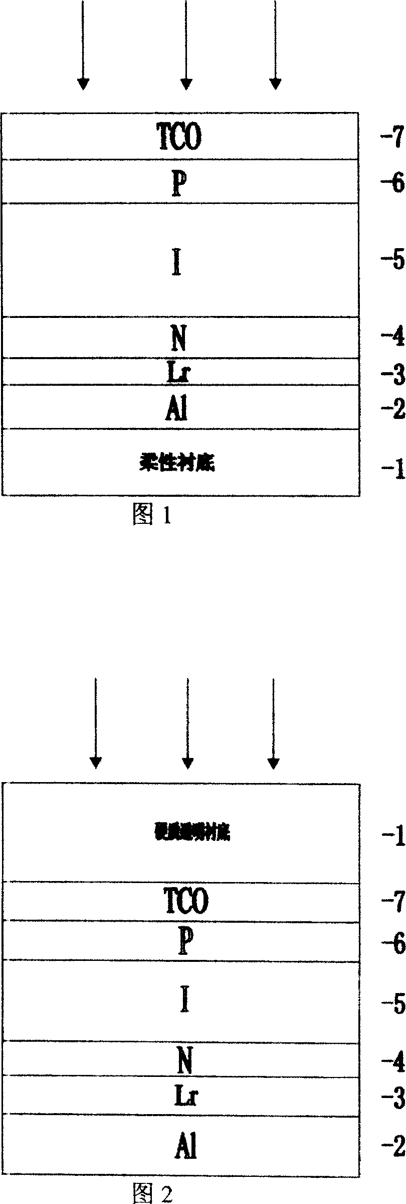
[0033] The structure of the flexible substrate thin film solar cell is shown in Figure 1. The main steps of the cell body are as follows:

[0034] The prepared polyimide flexible substrate with metal aluminum electrode, metal nickel (the thickness of nickel layer is about 40nm) or metal titanium barrier layer is put into the plasma enhanced chemical vapor deposition system, and the substrate is heated to 160 -180 ℃, and constant temperature for 2 hours; N, I, P three-layer silicon-based thin films were deposited in three different reaction chambers respectively. The reaction gases in the N chamber are silane, phosphine and hydrogen, the reaction power is 28W, and the film thickness is about 30nm; the reaction gases in the I chamber are silane, germane and hydrogen, the reaction power is 8W, and the film thickness is about 500nm; the P chamber reaction gas is Silane, borane, methane and hydrogen, the reaction power is 30W, and the film thickness is about 20nm. After the three-...

Embodiment 2

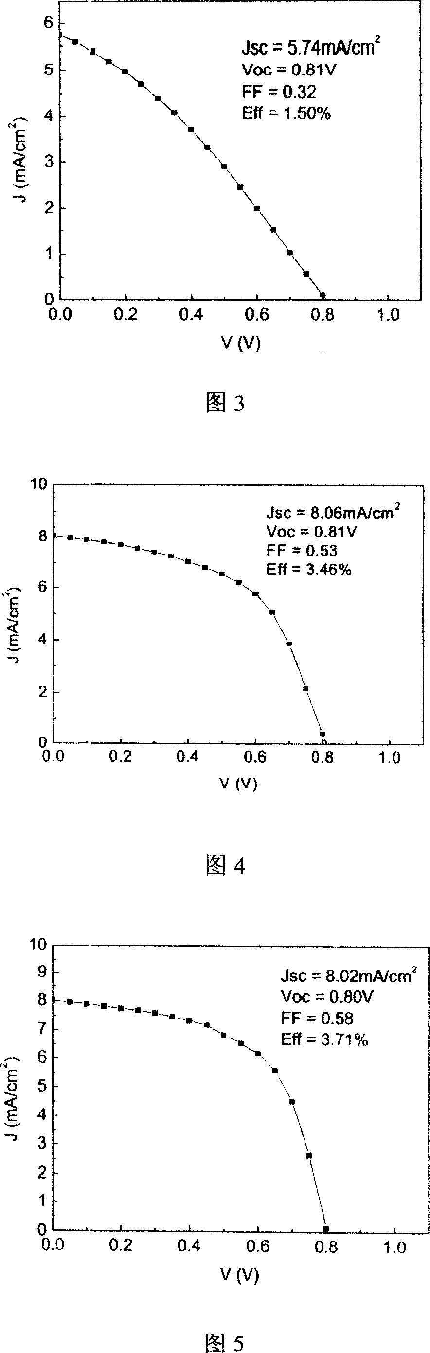
[0039] The structure of the transparent hard substrate thin film solar cell is shown in Figure 2. The main steps of the cell body are as follows:

[0040] The hard transparent substrate with the transparent conductive film was put into the plasma enhanced chemical vapor deposition system, and three layers of silicon-based films of P, I, and N were respectively deposited, and the experimental conditions were the same as those in Example 1. After cooling to room temperature, the solar cell was taken out from the plasma-enhanced chemical vapor deposition system, put into a coating machine to deposit a metal nickel or metal titanium barrier layer, and then metal aluminum was deposited. The experimental conditions were the same as in Example 1, except that the first deposition A metallic nickel or titanium barrier layer redeposits metallic aluminum. Take it out after cooling down, and the thickness of the barrier layer is about 45nm.


PUM

PropertyMeasurementUnit
thicknessaaaaaaaaaa
thicknessaaaaaaaaaa

Abstract

The barrier layer of thin film solar cell with a flexible substrate is composed of a metallic nickel layer or metallic titanium layer with 30-50nm thickness. It can prevent from metallic aluminum of back electrode entering into main body of cell at preparation of cell. Forming a barrier layer between back electrode and silicon-based film of cell doesní»t influence reflection of incident light, and meanwhile increases its light path action in absorbing layer of cell.

Description

technical field [0001] The present invention relates to a method for preparing a semiconductor thin film device with a flexible substrate, and more particularly, to a barrier layer of a thin film solar cell with a flexible substrate and a preparation method thereof. Background technique [0002] A solar cell is a device that directly converts light energy into electrical energy, among which silicon-based thin-film solar cells are the most widely used. Typically, silicon-based thin-film solar cells are deposited in the P-I-N order on glass substrates. The solar cell with flexible material as the substrate has low production cost, is easy to realize super-large area production, and is not limited by the area and shape in use. The polymer is light in weight, can be used as a battery substrate to obtain a high power-to-weight ratio, and can be bent arbitrarily. These advantages are beneficial to the application of solar cells in various special occasions such as satellites, sp...

Claims


Application Information

Patent Timeline
Patent Type & Authority Patents(China)
IPC IPC(8): H01L31/02H01L31/042H01L31/18C23C14/24H01L31/0216
CPCY02E10/52Y02P70/50
Inventor 张德贤蔡宏琨冯凯齐龙茵张晓赵飞李胜林
Owner NANKAI UNIV
Why Eureka
Try Eureka