Method for making base-board of liquid crystal display

A technology of liquid crystal display and manufacturing method, which is applied in semiconductor/solid-state device manufacturing, instrumentation, optics, etc., can solve the problems of simplifying the manufacturing process and not being able to meet the etching bevel angle at the same time, and achieve simplified manufacturing process, improved adhesion and electrical properties, The effect of reducing the production cost

Active Publication Date: 2009-05-20
AU OPTRONICS CORP
View PDF2 Cites 0 Cited by
  • Summary
  • Abstract
  • Description
  • Claims
  • Application Information

AI Technical Summary

Problems solved by technology

At present, there are ways to adjust the etching process parameters to control the formed inclination angle, such as using a special etchant in wet etching, or using special gases and process conditions in dry etching, but the current wet etching Or the process improvement of dry etching still cannot meet the requirements of good etching bevel, lower production cost, simplified process and mass production at the same time.

Method used


Image

  • Method for making base-board of liquid crystal display
  • Method for making base-board of liquid crystal display
  • Method for making base-board of liquid crystal display

Examples


Embodiment 1

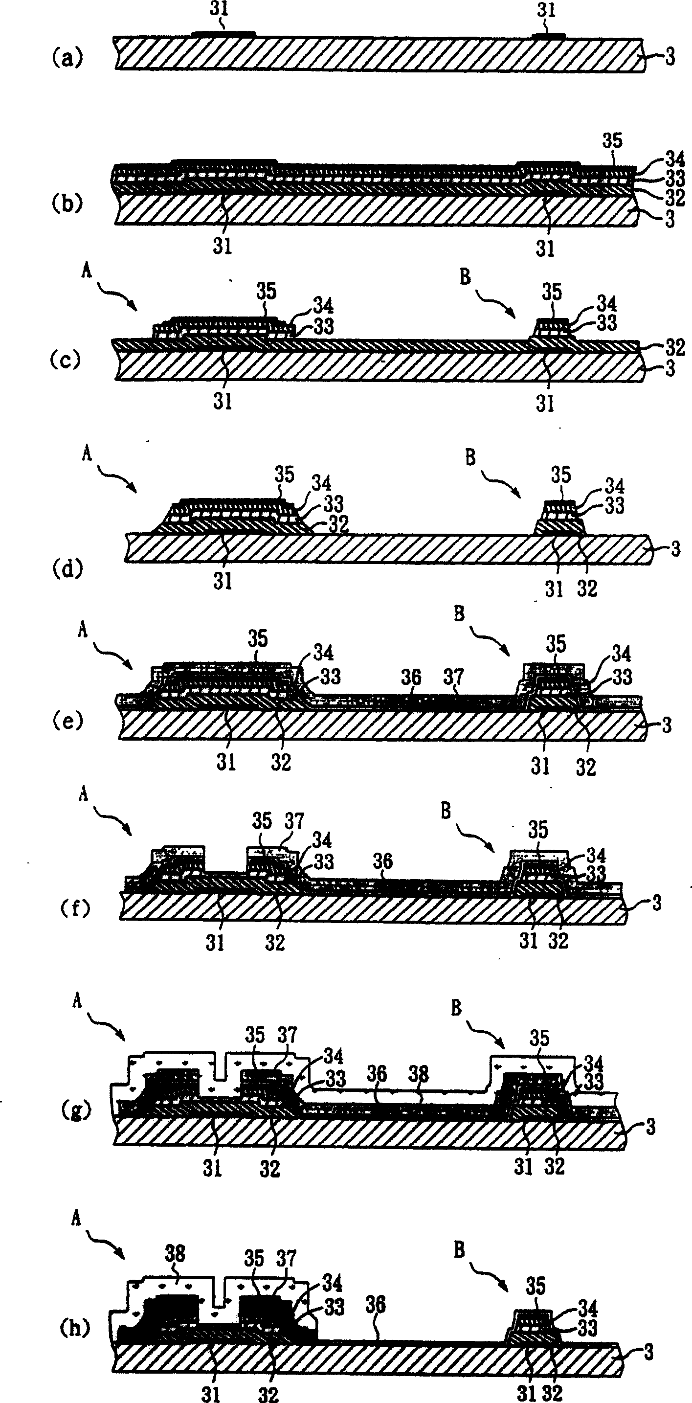
[0046] see image 3 Among (a) to (h), it is a flow chart of manufacturing the substrate for liquid crystal display in a preferred embodiment of the present invention, and the substrate for thin film transistor liquid crystal display manufactured in this embodiment adopts a four-pass photomask process.

[0047] Such as image 3 As shown in (a), first a transparent glass substrate 3 is provided, a first metal layer 31 is formed on the surface of the substrate 3, and a first yellow light and etching process is performed to complete the pattern of the gate layer. Wherein, the first metal layer 31 in this example is composed of chromium alloy and molybdenum metal, and its structure can be a single-layer or multi-layer structure (not shown in the figure).

[0048] Next, if image 3 As shown in (b), an insulating layer 32, a semiconductor layer 33, an ohmic contact layer 34, and a barrier layer 35 are deposited to cover the first metal layer 31; wherein the insulating layer 32 is a...

Embodiment 2

[0061] The manufacturing method of the substrate for the thin film transistor liquid crystal display of this embodiment is the same as the four-pass photomask process described in the first embodiment, except that the semiconductor layer is a multi-layer structure and the insulating layer etching conditions are adjusted, it is roughly similar to the embodiment. Content shown in Example 1.

[0062] The semiconductor layer of this embodiment is mainly composed of a multi-layer structure, wherein the semiconductor layer includes a low deposition rate silicon layer and a high deposition rate silicon layer to form a first metal layer / first insulating layer / low deposition rate on the surface of the substrate Multi-layer film structure of silicon layer / high deposition rate silicon layer / ohmic contact layer / barrier layer.

[0063] In this example, the high deposition rate of the silicon layer helps to reduce the deposition time of the semiconductor layer and increase the production ef...

Embodiment 3

[0072] The manufacturing method of the substrate for the thin film transistor liquid crystal display of this embodiment is the same as the process conditions described in the second embodiment, which is also a four-pass photomask process. Except that the semiconductor layer adopts the single-layer structure of the first embodiment, the remaining process conditions, such as : The etching gas and the interlayer structure of other film layers of the thin film transistor are roughly similar to those shown in the second embodiment.


PUM


Abstract

This invention discloses a method for manufacturing a base plate of a LCD used in improving the etched tilt angles of a semiconductor layer and an insulation layer, which utilizes an etching gas containing FS compound to etch the insulation layer to form a fine etched tilted angle and the semiconductor layer can have a side etched result to increase the coverage of the ladder to the latter process, which can process film transistors in many layers of structures containing a block layer, a semiconductor layer and an insulation layer without peeling off the layers.

Description

technical field [0001] The invention relates to a method for manufacturing a thin film transistor, especially a method for manufacturing a substrate suitable for liquid crystal displays. Background technique [0002] The TFT-LCD is mainly composed of a TFT array substrate, a color filter array substrate, and a liquid crystal layer, wherein the TFT array substrate is composed of a plurality of TFTs arranged in an array and a pixel electrode corresponding to each TFT composed of multiple pixel structures. It is known that six or five photomasks are often used to fabricate thin film transistor array substrates, and the fabrication process generally includes defining gates, active regions, sources and drains, connection pad openings, and pixel regions in sequence. Due to the lengthy fabrication process And complex, not only expensive, but also easy to cause problems such as process defects, so how to reduce the number of photomasks and simplify the number of processes has becom...

Claims


Application Information

Patent Timeline
Patent Type & Authority Patents(China)
IPC IPC(8): H01L21/84H01L21/311G02F1/136
Inventor 詹勋昌李佳宗郭可欣
Owner AU OPTRONICS CORP
Why Eureka
Try Eureka