

Emitting laser for etching top end non-doping intrinsic layer asymmetric metal membrane vertical cavity surface
A technology of vertical cavity surface emission and lasers, which is applied in the direction of lasers, laser components, semiconductor lasers, etc., can solve the problems of inability to realize small current apertures, uncontrollable small apertures of separate oxidation, and limit development, so as to improve the photoelectric coupling efficiency. , Improve luminous efficiency, reduce the effect of regional recombination
- Summary
- Abstract
- Description
- Claims
- Application Information
AI Technical Summary
Problems solved by technology
Method used
Image

Examples
Embodiment Construction
[0039] The present invention is described in detail below in conjunction with accompanying drawing:
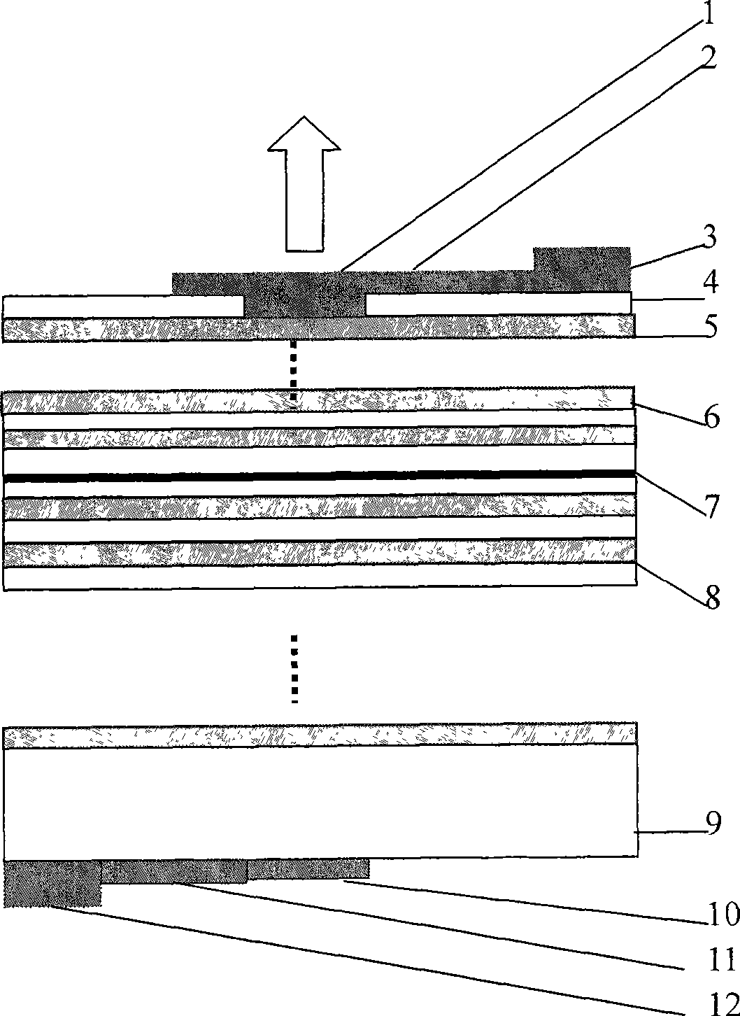
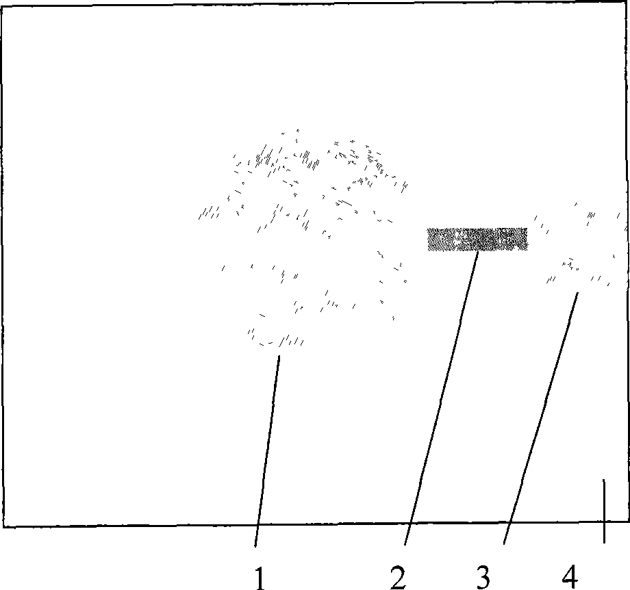
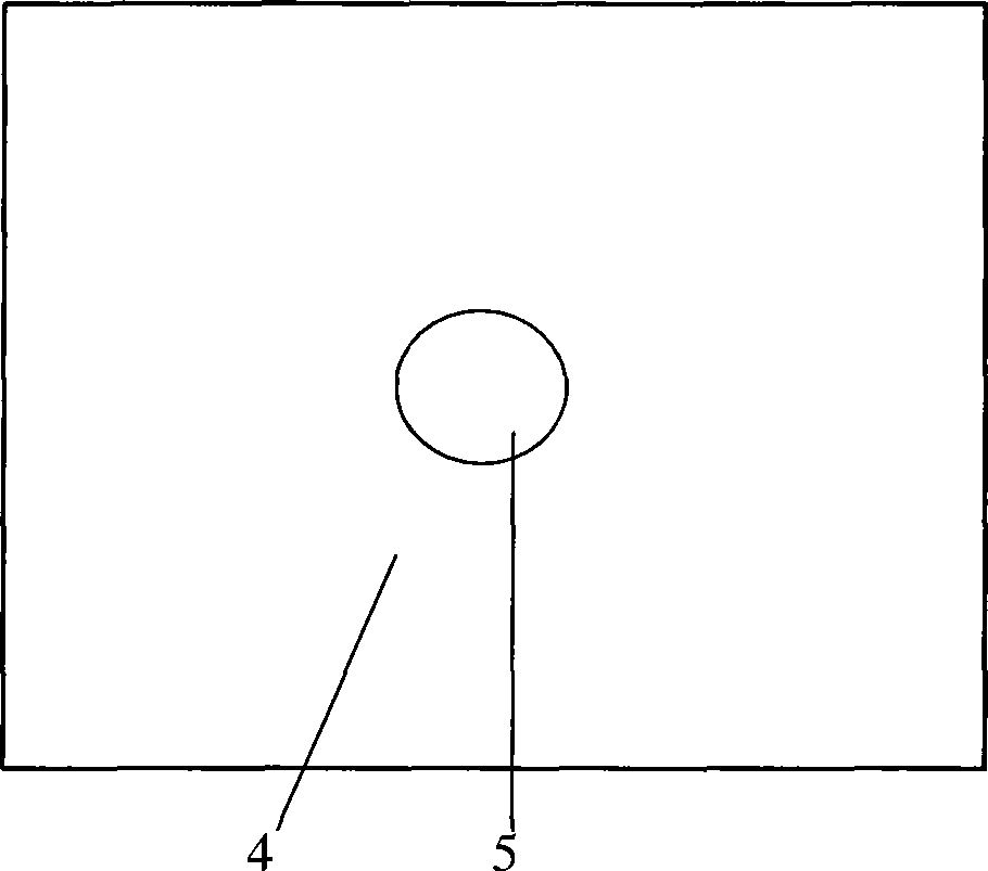
[0040] as the picture shows, figure 1 It is a structural schematic diagram of the product of the present invention; figure 2 The top view of the upper electrode and the top metal film etching area of the vertical cavity surface emitting laser with etched metal film; image 3 Top view of the undoped intrinsically high-resistance region of the etched current aperture, Figure 4 Bottom view of the bottom electrode and the etched area of the metal-plated film of the etched metal film vertical cavity surface emitting laser.
[0041] Among them, 1: the circular metal reflective film etched on the upper surface, with a radius of 4 to 8 microns; 2: the metal film wire etched on the upper surface; 3: the metal film and electrode in contact with the etched electrode on the upper surface; Doped intrinsically high resistance semiconductor material, the radius of the hole is 1-2 mi...
PUM
| Property | Measurement | Unit |
|---|---|---|
| radius | aaaaa | aaaaa |
| radius | aaaaa | aaaaa |
Abstract
Description
Claims
Application Information