High-performance semiconductor nanometer silicon field electronic emission material and its preparation method

A field electron emission and semiconductor technology, which is applied in semiconductor/solid-state device manufacturing, nanostructure manufacturing, nanotechnology, etc., can solve the problems of large open electric field and low field emission current density, so as to improve the electric field intensity and facilitate large-scale production , the effect of simple process

Inactive Publication Date: 2007-08-15
NANJING UNIV
View PDF0 Cites 7 Cited by
  • Summary
  • Abstract
  • Description
  • Claims
  • Application Information

AI Technical Summary

Problems solved by technology

However, as a field electron emission material, it is not an ideal choice, mainly due to the large turn-on electric field of this material and the low field emission current density

Method used


Image

  • High-performance semiconductor nanometer silicon field electronic emission material and its preparation method
  • High-performance semiconductor nanometer silicon field electronic emission material and its preparation method

Examples


Embodiment 1

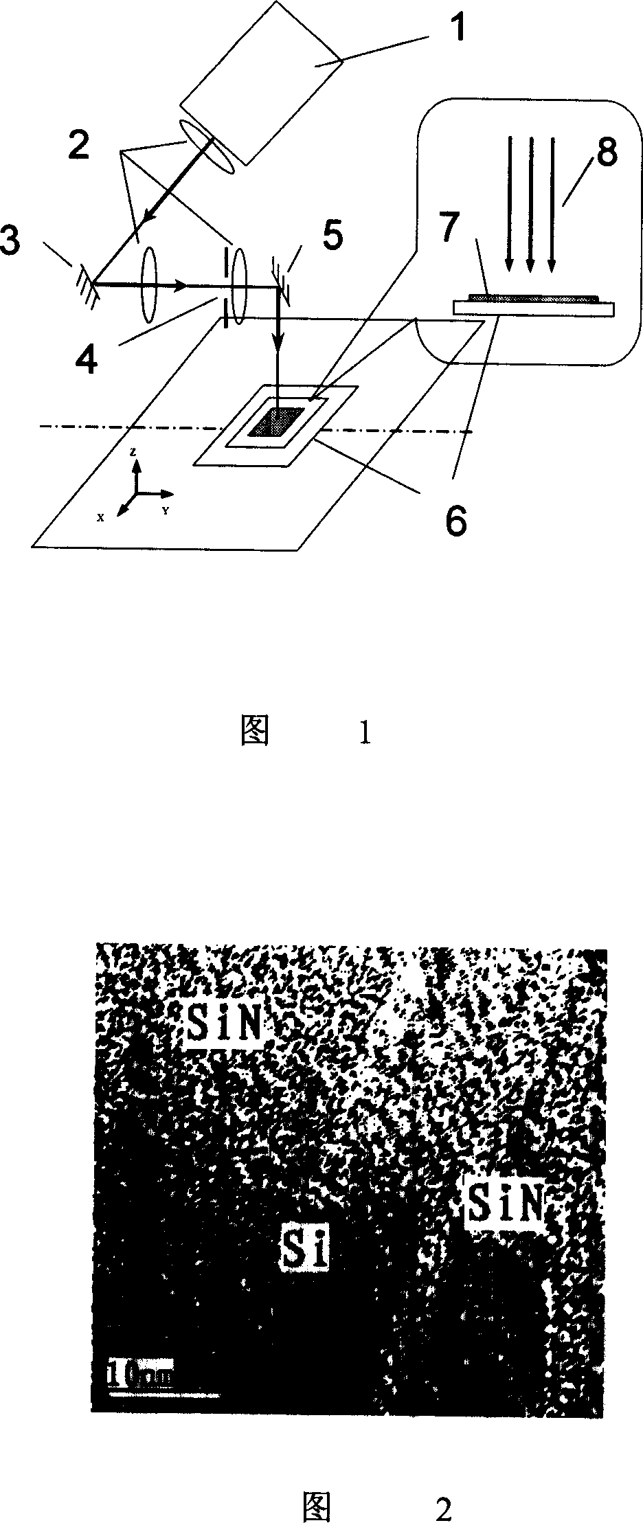
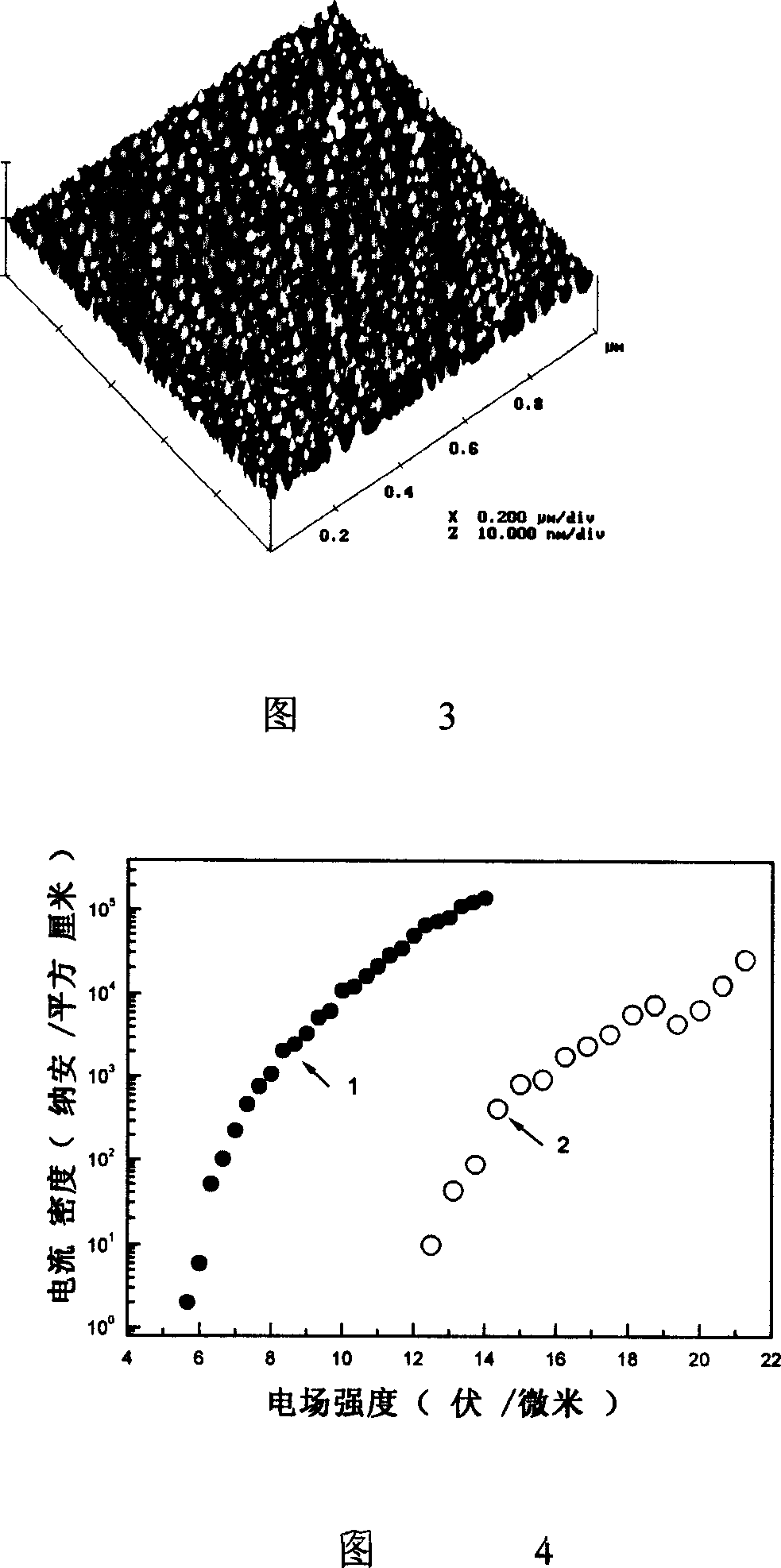
[0035] This embodiment adopts the following process to prepare high-performance semiconductor silicon field electron emission material:

[0036] 1. Preparation of hydrogenated amorphous silicon (a-Si:H) thin film: use flat capacitive radio frequency plasma enhanced chemical vapor deposition (PECVD) system (for example: Plasmalab system100 of Oxford Instrument Company, China, Shenyang Science and Instrument Center of Chinese Academy of Sciences in China PECVD-X equipment is on the stage, usually the power source frequency is 13.56MHz, and the power is 30W) to deposit hydrogenated amorphous silicon semiconductor film on the substrate.

[0037] The film can be deposited on a heavily doped n-type Si (100) substrate covered with an amorphous silicon nitride film, or on a glass substrate or other substrates evaporated with a metal film.

[0038] During deposition, the substrate is placed on the grounded anode electrode of the reaction chamber, and the reaction gas is silane (SiH 4 ...


PUM

PropertyMeasurementUnit
thicknessaaaaaaaaaa
particle diameteraaaaaaaaaa
thicknessaaaaaaaaaa

Abstract

The related semi-conductor silicon field electronic emission material comprises: a 4-50nm hydrogenized amorphous silicon semi-conductor film deposited on substrate, and 1-10nm silicon grains distributed evenly. The preparation method comprises depositing, and quasi-molecular ultrashort pulse laser crystallizing. This product has low field-emission threshold and high field enhancing factor, and important to semi-conductor material application in large-area plane display.

Description

technical field [0001] The invention relates to a field electron emission material, especially a semiconductor silicon nanometer field electron emission material, and also relates to a preparation method thereof, which belongs to the technical field of semiconductor materials. Background technique [0002] In today's information society, the requirements for information display technology are getting higher and higher. The traditional cathode ray tube (CRT) is far from being able to meet people's requirements. It has become one of the main development directions in display technology to replace huge and bulky cathode ray tubes with flat panel displays, and to develop lightweight and miniaturized ultra-thin computer display devices and televisions. In this regard, countries all over the world have invested a lot of manpower and material resources in research and development, and thin-film transistor liquid crystal display devices, plasma display devices, etc. are gradually r...

Claims


Application Information

Patent Timeline
Patent Type & Authority Applications(China)
IPC IPC(8): H01J1/304H01J9/02H01L21/205H01L21/324B82B1/00B82B3/00C30B29/00
Inventor 徐骏陈坤基黄信凡徐岭李伟马忠元
Owner NANJING UNIV
Why Eureka
Try Eureka