P-type nitrogen-doping cuprous oxide thin film material and preparation method thereof

A cuprous oxide, thin-film material technology, applied in metal material coating process, semiconductor/solid-state device manufacturing, ion implantation plating, etc. High-level problems, to achieve the effect of simple manufacturing process, increased hole concentration, and high hole concentration

Inactive Publication Date: 2007-10-24
HANGZHOU DIANZI UNIV
View PDF0 Cites 24 Cited by
  • Summary
  • Abstract
  • Description
  • Claims
  • Application Information

AI Technical Summary

Problems solved by technology

However, it is difficult to obtain pure cuprous oxide phases by common film preparation methods, so there are more or less copper oxide phases in cuprous oxide films.
Since cuprous oxide is a P-type hole-conducting semiconductor material, and copper oxide is an N-type

Method used


Image

  • P-type nitrogen-doping cuprous oxide thin film material and preparation method thereof
  • P-type nitrogen-doping cuprous oxide thin film material and preparation method thereof

Examples


Embodiment 1

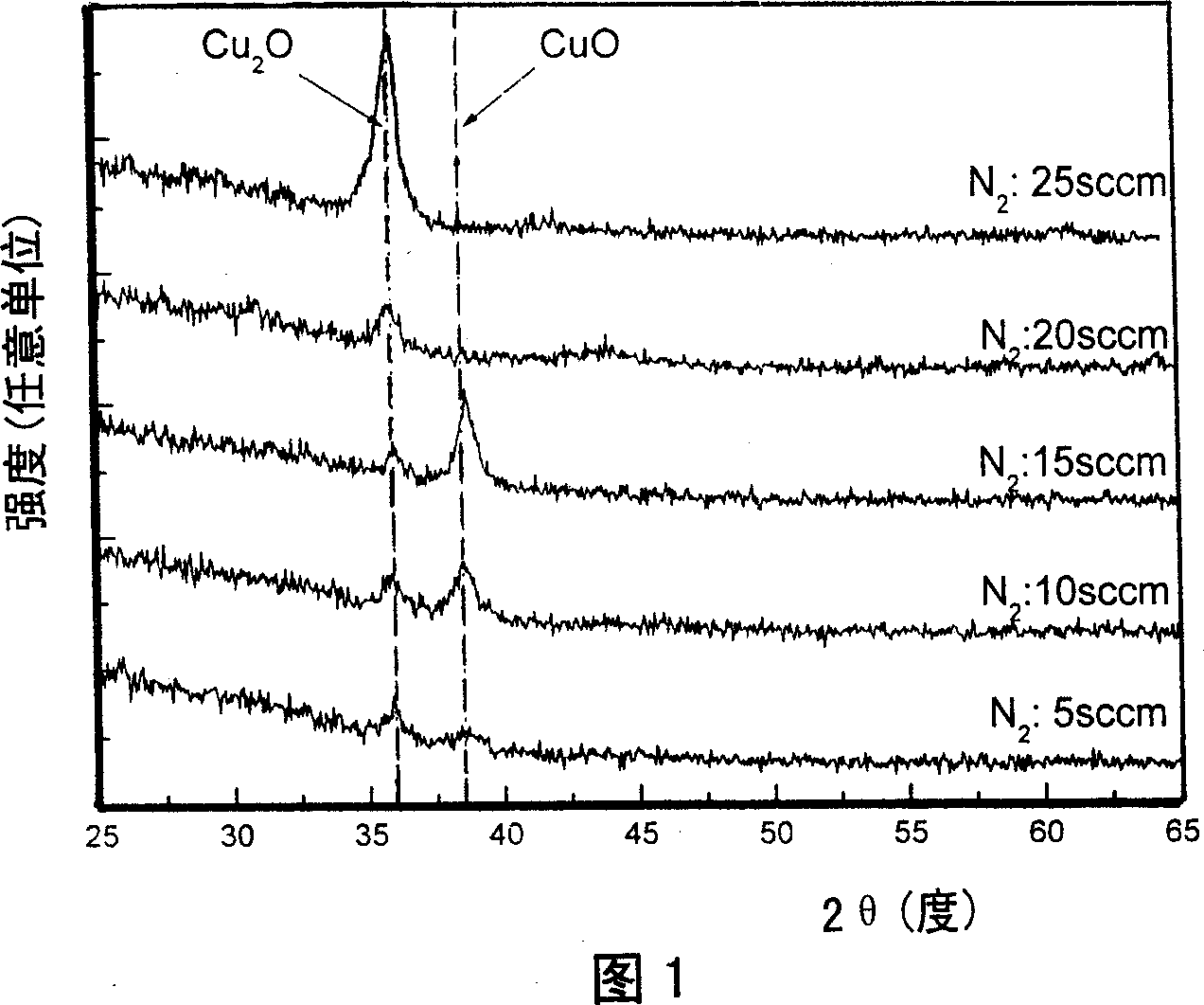
[0013] A kind of P-type nitrogen-doped cuprous oxide film material, its molecular formula is Cu 2 O:N, the deposition process is as follows: 1) The target material is a copper disc with a purity of 99.99%, a thickness of 3.6mm, and a diameter of 50mm. The purity is 99.999%; 2) The distance between the magnetron sputtering target and the substrate is 5cm, and the back-bottom pressure of the deposition chamber is 1.2×10 -3 Pa. During deposition, the substrate temperature is normal temperature, the flow rates of oxygen, nitrogen, and argon are 20, 30, and 80 sccm respectively, and the working pressure in the deposition chamber is controlled to 1.0 Pa by adjusting the valve; 3) The sputtering voltage is 400V, and the current is 50mA , the power is 20W; the film deposition time is 20 minutes.

[0014] The results of the Hall effect test show that the resistivity of the thin film material is 1.2 Ω cm, and the hole concentration is 3.8×10 19 / cm 3 .

Embodiment 2

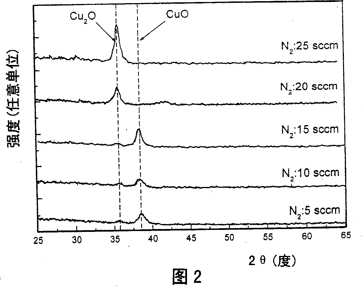
[0016] A P-type nitrogen-doped cuprous oxide thin film material is characterized in that: the thin film material is nitrogen-doped cuprous oxide, and its molecular formula is Cu 2 O:N. The deposition process is as follows: 1) The target material is a copper disc with a purity of 99.99%, a thickness of 3.6mm, and a diameter of 50mm. %. 2) The distance between the magnetron sputtering target and the substrate is 5cm, and the back pressure of the deposition chamber is 1.2×10 -3 Pa. During deposition, the substrate temperature was 100°C, the flow rates of oxygen, nitrogen, and argon were 20, 30, and 80 sccm respectively, and the working pressure in the deposition chamber was controlled to 1.0 Pa by adjusting the valve; 3) The sputtering voltage was 400V, and the current was 50mA, power 20W; film deposition time 20 minutes. The test results show that the resistivity of the thin film material is 4.07Ω·cm, and the hole concentration is 4.0×10 19 cm -3 .


PUM

PropertyMeasurementUnit
Resistivityaaaaaaaaaa
Hole concentrationaaaaaaaaaa
Resistivityaaaaaaaaaa

Abstract

The invention discloses a P-typed doped cuprous oxide film material, which comprises the following steps: setting the doped density of nitrogen in the film at 1X1015cm-3-5X1019cm-3 with one cuprous oxide phase and molecular formula at Cu2O: N; adopting DC reacting magnetic control sputtering method to prepare, common carrier as substrate, red copper disc with purity at 99. 99% as target material; setting argon gas and oxygen, nitrogen as the working gas and reacting gas separately with gas purity at 99. 999%; making the flow rate of oxygen and nitrogen at 3: 2 and the bottom pressure of sediment chamber at 1. 2X10⁻³Pa-1. 0Pa; setting the substrate temperature between normal temperature and 100 deg. c and sputtering pressure at 400V with current at 50mA and power at 20W; depositing the film for 20min.

Description

technical field [0001] The invention relates to a P-type nitrogen-doped cuprous oxide film material and a manufacturing method thereof. Background technique [0002] With the further increase in the demand for environmentally friendly and renewable energy, people's interest in solar energy utilization has increased rapidly. Especially in recent years, the photovoltaic conversion technology that uses semiconductor thin film materials to directly convert solar energy into electrical energy has attracted many people's attention. . At present, in addition to silicon materials, the materials used for solar cells include copper indium selenide, gallium arsenide, copper indium gallium selenide, etc. These materials are very expensive because of the raw materials, or because of the complicated manufacturing process, or the existence of toxicity, serious environmental pollution, etc. defect. [0003] Cuprous oxide is an ideal photovoltaic material. Its forbidden band width is 2.14e...

Claims


Application Information

Patent Timeline
IPC IPC(8): C03C17/245C23C14/08C23C14/35H01L21/203H01L31/00
Inventor 季振国张亚红
Owner HANGZHOU DIANZI UNIV
Why Eureka
Try Eureka