Method for making groove power semiconductor device

A device manufacturing method and power semiconductor technology, which are applied in semiconductor/solid-state device manufacturing, semiconductor devices, electrical components, etc., can solve the problems of increasing process complexity, device performance degradation, and source region junction depth, etc., to improve switching characteristics, The effect of increasing the breakdown strength and reducing the electric field strength

Inactive Publication Date: 2008-01-09
HARBIN ENG UNIV
View PDF1 Cites 24 Cited by
  • Summary
  • Abstract
  • Description
  • Claims
  • Application Information

AI Technical Summary

Problems solved by technology

As described in the published U.S. patent document (US6,262,453 B1), utilize partial exposure to fill in the photosensitive glue in the groove and form thick oxide layer at the bottom of the groove, this method needs to strictly control the exposure condition of the photosensitive glue, and clear the groove The bottom photosensitive glue increases the complexity of the process
In addition, as the cell size of the device is further reduced, the junction depth of the source region becomes very shallow. At this time, the so-called "metal nail" will enter or penetrate the source region, deteriorating or even failing the device performance.

Method used


Image

  • Method for making groove power semiconductor device
  • Method for making groove power semiconductor device
  • Method for making groove power semiconductor device

Examples


Embodiment 1

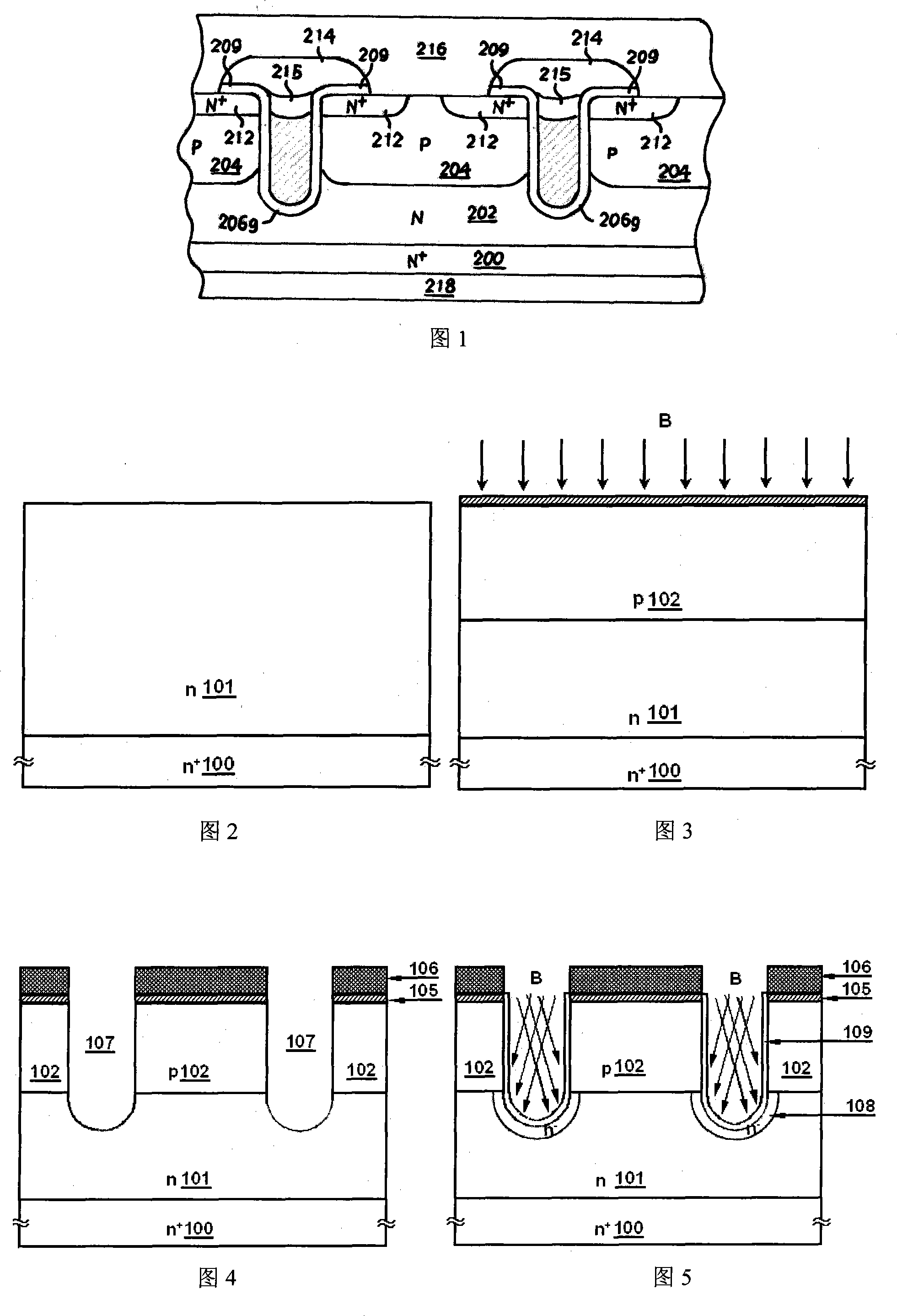
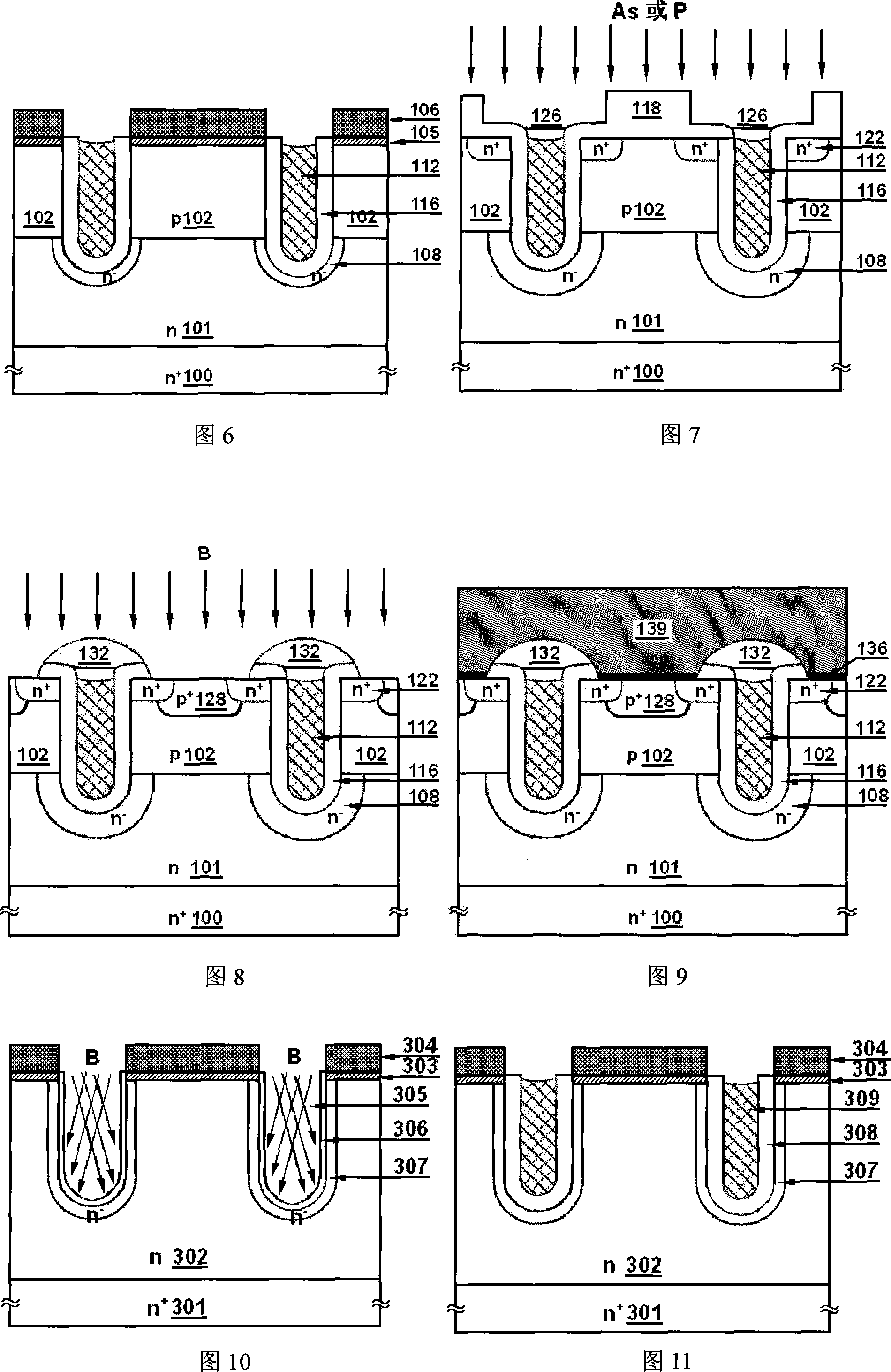
[0051] In conjunction with Figures 2-9, the specific steps of this embodiment are:

[0052] (1) Base preparation, in n + or p + Epitaxial growth on substrate n - Area;

[0053] (2) Utilize the LPCVD method to grow a thin oxide layer on the semiconductor substrate obtained in step (1), and the film thickness is controlled at 500 angstroms;

[0054] (3) Perform ion implantation of B impurities on the surface of the semiconductor substrate obtained in step (2), the ion implantation energy is typically 600KeV, and the implantation dose is controlled at 10 14 cm -2 ;

[0055] (4) utilize LPCVD method to grow Si at the semiconductor substrate surface of step (3) gained 3 N 4 , the thickness is controlled at 800 Angstroms;

[0056] (5) Spin-coat photosensitive adhesive on the surface of the semiconductor substrate obtained in step (4), obtain a groove etching window through a photolithography process, and form a groove structure by combining dry etching and wet etching;

[0...

Embodiment 2

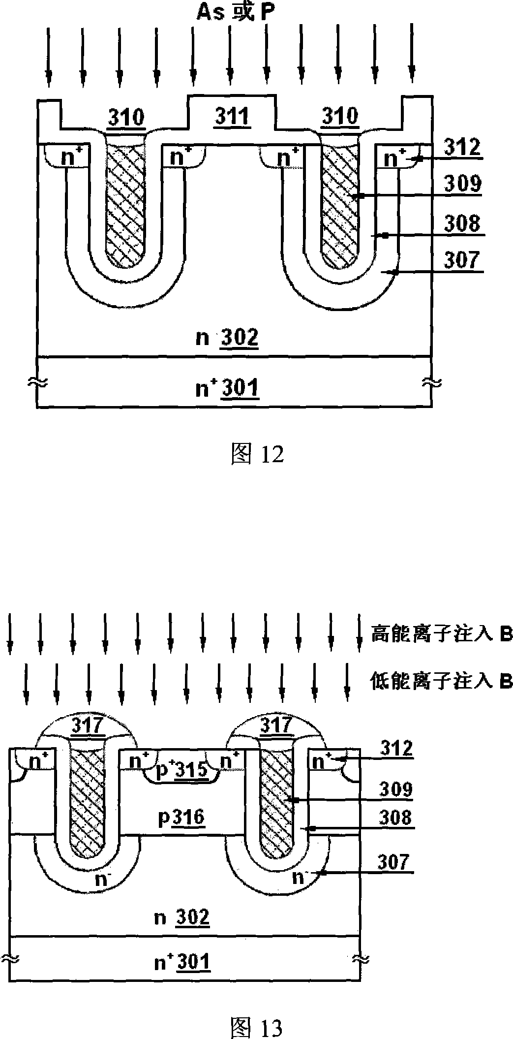
[0071] Referring to FIG. 10 , an epitaxial layer 302 is grown on an n+ substrate 301 with a resistivity of 0.003Ω·cm, and the thickness of the epitaxial layer depends on the requirements of the device for withstand voltage and on-resistance. On the surface of the epitaxial layer 302, LPCVD sequentially grows SiO with a thickness of 1000 Ȧ 2 layer 303 and Si with a thickness of 600 Å 3 N 4 Layer 304. Form the etching window of the trench gate through the photolithography process, adopt anisotropic etching such as RIE to form the trench 305, and supplemented by wet etching (in this embodiment, dilute HNO 3 , HF and H 2 O mixture). SiO with a thickness of 1300 Ȧ was grown by LPCVD on the inner surface of the trench of the above-mentioned substrate 2 The sacrificial layer 306 is grown under the implantation energy of 100KeV, with 5*10 11 cm -2 The dose of B is injected into B, and the n-region 307 is formed by diffusion at a high temperature of 1100° C. for 100 minutes.

...


PUM


Abstract

The invention is concerned with the manufacture method of the ditch groove power semiconductor device. It is: provides the materials of the basal; forms the first electric transmit epitaxy layer on the basal; forms the second electric transmit zone and the ditch groove inside the epitaxy layer; forms the ebb first electric transmit area and the medium layer with the ditch groove; and then, forms the electric transmit area within the medium layer; forms the first electric transmit source area on the surface of the second electric transmit area; forms the second electric transmit contact area with higher doping PH indicator on the second electric transmit zone surface; forms the passivation layer cap on the top of the ditch groove which must with the medium layer and the electric transmit area; forms the diffusion protecting layer on the surface of the source area and the contact area; finally, forms the structure surface with good electric connection. The invention can control the threshold voltage of the device and improves the breakdown strength of the oxide layer of the device bottom area, and improves its electric connection reliability with no extra cover film printing plate and complex method request.

Description

(1) Technical field [0001] The invention belongs to the field of semiconductor device manufacturing, in particular to a method for manufacturing a trench gate power semiconductor device. (2) Background technology [0002] In the field of power electronics, power semiconductor devices are key components, and their performance characteristics play a major role in improving system performance. In order to achieve better performance, for example, lower on-state resistance is required for power MOS devices, the technology has rapidly developed from the technology of a few microns to deep sub-micron twenty years ago. For the traditional MOS structure, modern technological progress has reached the point where the size of the MOS cell can be reduced and the on-resistance cannot be reduced, which makes it difficult to reconcile the contradiction between high breakdown voltage and low on-resistance. The appearance of the trench structure can also effectively solve the on-resistance p...

Claims


Application Information

Patent Timeline
Patent Type & Authority Applications(China)
IPC IPC(8): H01L21/336H01L21/28
Inventor 王颖赵旦峰曹菲程超
Owner HARBIN ENG UNIV
Why Eureka
Try Eureka