

Epitaxy growth method for gallium antimonide on gallium arsenide substrate
A technology of epitaxial growth and gallium arsenide, applied in the field of epitaxial growth of gallium antimonide crystal, can solve the problems of rough surface, poor crystal quality and high dislocation density of GaSb material, and achieve the improvement of crystal quality, surface flatness, and smooth surface. The effect of increasing the degree of dislocation and decreasing the dislocation density
- Summary
- Abstract
- Description
- Claims
- Application Information
AI Technical Summary
Problems solved by technology
Method used
Image

Examples
Embodiment 1
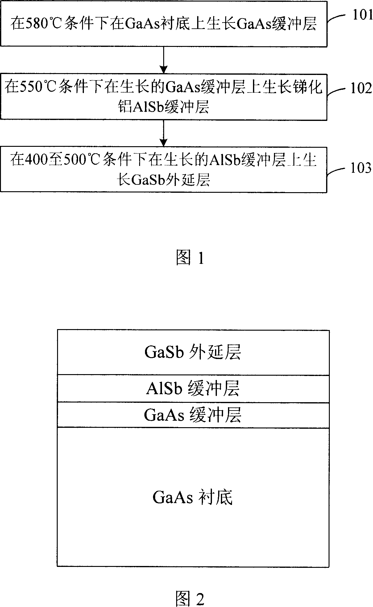
[0055] After high-temperature deoxidation and degassing of the cleaned GaAs substrate, the temperature of the GaAs substrate is lowered to 580°C, the Ga source furnace shutter is opened, the Ga source temperature is 1150°C, and the GaAs high-temperature buffer layer is crystallized on the GaAs substrate grow. The growth time of the GaAs buffer layer is 30 minutes, and the thickness is 0.5 μm.
[0056] Then close the Ga source furnace shutter, lower the substrate temperature to about 550°C, close the As source furnace shutter, open the Sb source furnace shutter, open the Al source furnace shutter, the Al source temperature is 1180°C, and grow a low-temperature AlSb buffer on the GaAs buffer layer. layer, the growth time is 12 minutes, and the thickness is about 100nm.
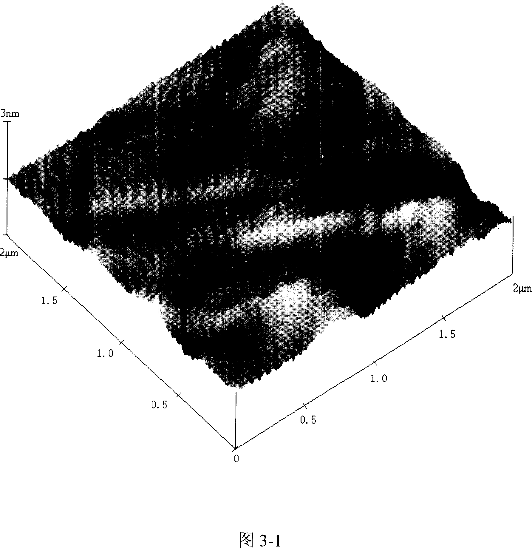
[0057] Then close the shutter of the Al source furnace, lower the substrate temperature to 500°C, open the shutter of the Ga source furnace, and grow the epitaxial layer GaSb on the AlSb buffer layer. The surfa...
Embodiment 2、3
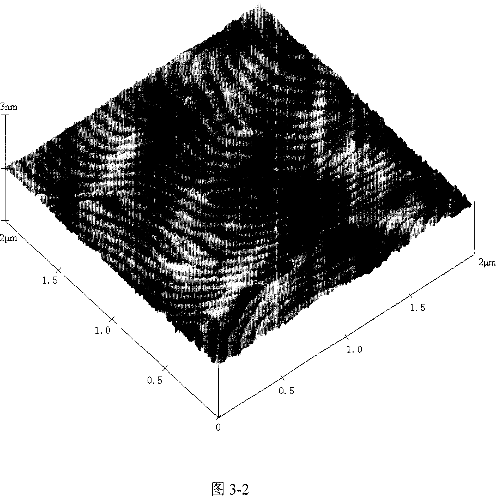
[0059] The epitaxial layer growth temperatures at lower temperatures were 460° C. and 480° C., and the rest were the same as in Example 1. The surface roughness measured by the atomic force microscope and the FWHM value measured by the DCXRD rocking curve are listed in Table 1.
[0060] Example
[0061] Table 1
PUM
 Abstract
Description
Claims
Application Information