Nanometer array and method for forming the same

A nano-array and nano-technology, applied in the direction of nano-technology, nano-technology, nano-structure manufacturing, etc., can solve the problems of nano-structure damage, polymer structure deformation, high process cost, etc.

Inactive Publication Date: 2008-05-14
IND TECH RES INST
View PDF6 Cites 28 Cited by
  • Summary
  • Abstract
  • Description
  • Claims
  • Application Information

AI Technical Summary

Problems solved by technology

[0005] Korean patent KR20030784279Woo Lee et al. used AAO templates as the basis to describe the replication of four nanostructures, in which aluminum was anodized into a porous alumina structure, and templates with different hole sizes were produced according to different hole expansion conditions. Polymer replication molding, the template is etched and removed to obtain a nano-cylindrical structure of the polymer, or the microstructure holes on the upper layer of the template are etched and removed to form a secondary aluminum template. The secondary template can be used to replicate the nanostructured film with the polymer solution. The microstructure template can also be copied by electroforming. In addition, this patent also points out that the surface is coated with inorganic nanoparticles, and then coated with a layer of polymer solution. After the solvent evaporates, the surface has irregularly distributed nanoparticles. Composite nanostructure polymer film, this patent not only uses the structure of AAO itself as the replication template, but also uses the aluminum on the bottom plate after AAO removal as the secondary template, and also uses the molten polymer solution as the replication material. After filling, the solvent must be removed, and the template can not be directly separated from the formed polymer membrane by etching the template, which will cause deformation of the polymer structure during the process, and the nanostructure of the secondary template will be different from that of the AAO template. If the nanostructure is too different, the function of the nanostructure of the replicated polymer module will be different, or even destroyed.
[0006] In DE10154756, it is proposed to use the microstructured oxide coating on the surface as a template for nanostructure imprinting to carry out compression molding of nano-columnar bodies. The template itself is not hollow and can easily produce nanometers with regular surfaces by molding. Structure, the nanostructure configuration formed by this method will be consistent with the nano-template, that is, the shape of the template is completely copied, so a nano-template has only one nano-configuration, and the configuration change cannot be adjusted according to the process conditions, and the surface layer is shaped The nanostructure of the film is quite fragile. If there is no interface treatment during the film removal, the formed nanostructure will be damaged. Without strengthening treatment of the surface nanostructure, it will cause problems during use.
[0007] U.S. Patent Early Publication 2004188874 is a multilayer coating of polymer film anti-reflection structure. The surface is coated with a layer of high-reflection particles, and ripples are formed on the surface by mold replication. The hardened layer is coated on the polymer film. The combination of concave-convex structure and high-reflectivity particles can have anti-glare and low-reflection functions. This optical functional layer is still composed of wavy lines with a period of tens of μm on the surface and high-refractive particles. The hardened layer that provides support is in the optical functional layer. Below, the bottom is the polymer film substrate. The multi-layer structure will have the problem of interface refractive index and bonding strength. The different thermal expansion coefficients between layers must be considered, which will be required in environmental testing and use. Especially to solve, so the process difficulty is high, and the process cost is relatively high

Method used


Image

  • Nanometer array and method for forming the same
  • Nanometer array and method for forming the same
  • Nanometer array and method for forming the same

Examples


Embodiment Construction

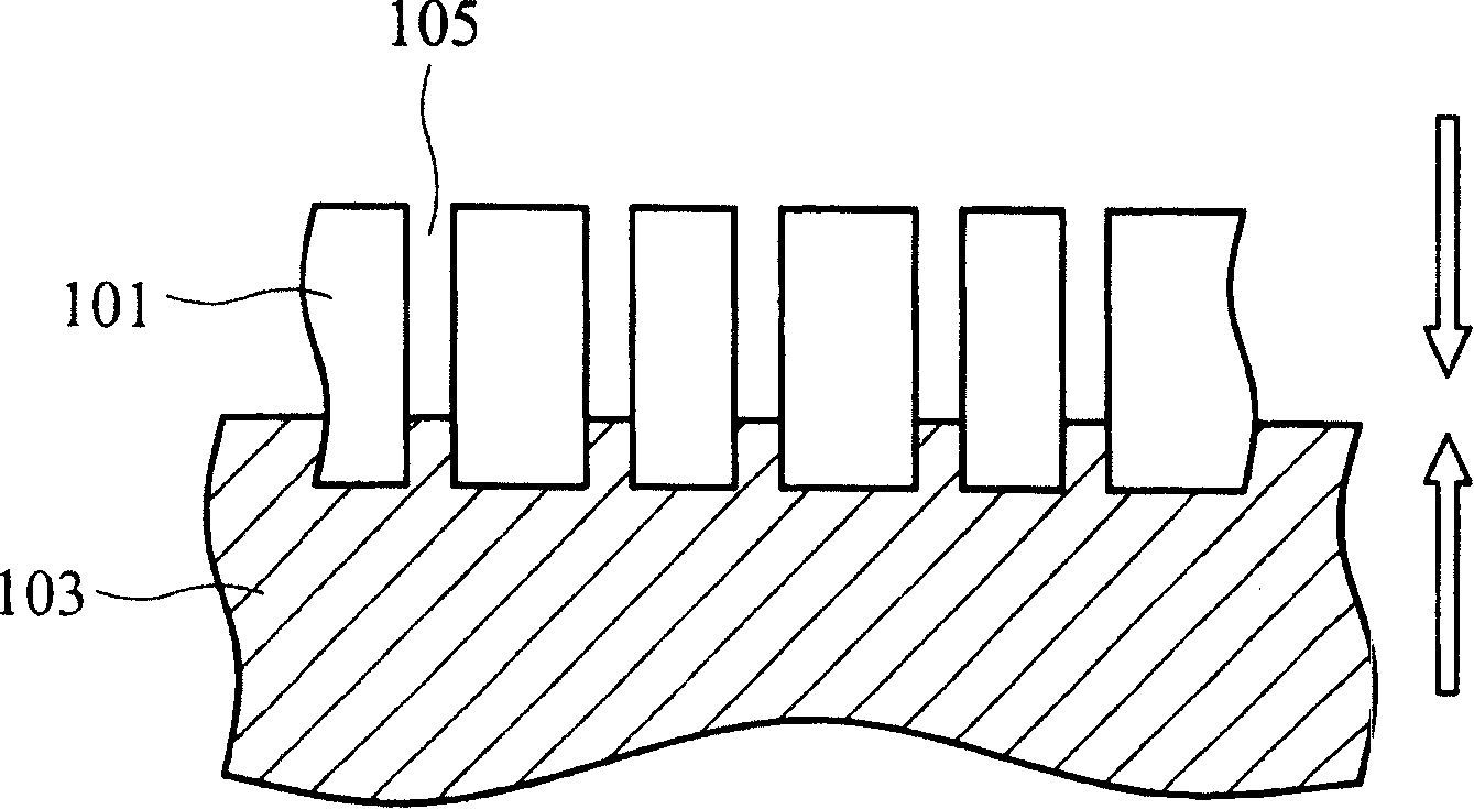
[0036] The invention utilizes the concept of polymer film imprinting and can be widely used in thermoplastic polymer materials without melting the polymer materials in organic solvents, avoiding structural deformation and environmental protection problems caused by solvent removal and solvent volatilization in the future.

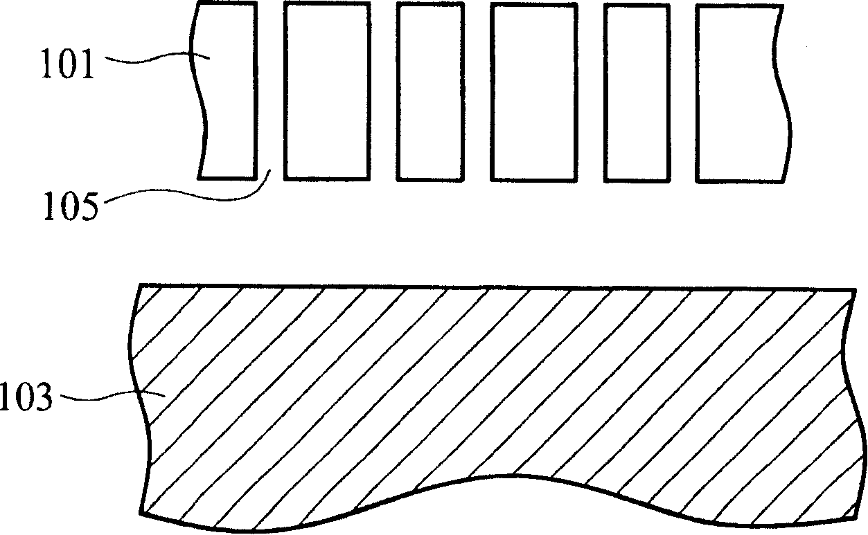
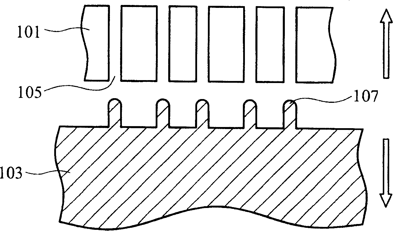
[0037] Figure 1 to Figure 3 It shows the flow chart of the present invention using the hot-pressing nano-imprinting method and using porous anodized aluminum as the imprinting template to form the nano-array. Such as figure 1 As shown, the aluminum oxide template 101 is formed by anodizing pure aluminum and has a plurality of nano-holes 105. Secondary anodizing can also be used to increase the uniformity of the nano-hole diameter, so as to precisely control the nano-pores formed after the imprinting process. The error of the array diameter, in one embodiment, the diameter of the nanoholes is about less than 200 nm, preferably between about 20 nm and 150 nm. ...


PUM

PropertyMeasurementUnit
thicknessaaaaaaaaaa
thicknessaaaaaaaaaa
thicknessaaaaaaaaaa

Abstract

The invention provides a method forming nanometer array, which comprises a template with a plurality of nanometer holes; which is characterized in that pressing art is performed on a macromolecule base material for the template; the template is stripped, thereby a plurality of bulges on the macromolecule base material are formed.

Description

Technical field [0001] The present invention relates to a method for forming a nanoarray, and more particularly to a method for forming a nanoarray by imprinting. Background technique [0002] The regular nano-structured surface has special effects, such as compound eye structure with ultra-low reflectivity moth eye, insect wing structure resistant to dust adhesion, lotuse effect of hydrophobic self-cleaning lotus leaf surface, etc. The scale is about 100nm The structure has special properties. How to apply the functions of these nanostructures in daily life is the goal of the development of nanotechnology. Generally, if polymers want to achieve hydrophobic self-cleaning, oil resistance or reflectivity reduction, they must undergo secondary surface chemical or physical treatment to obtain the above-mentioned functions. The process is quite complicated and expensive, and a variety of chemistries must be used. Product or additional equipment. Taking photolithography technology as a...

Claims


Application Information

Patent Timeline
Patent Type & Authority Applications(China)
IPC IPC(8): B82B1/00B82B3/00B29C59/02B29C33/56
Inventor 赵志强萧柏龄赖美君
Owner IND TECH RES INST
Why Eureka
Try Eureka