Method for producing large area polysilicon

A polysilicon, large-area technology, applied in polycrystalline material growth, chemical instruments and methods, crystal growth, etc., can solve the problems of large-area uniformity and poor repeatability, high cost of laser equipment, small irradiation area, etc., to achieve crystallization Short conversion time, ensuring uniformity and repeatability, and good radiation uniformity

Active Publication Date: 2008-06-11
余建军
View PDF0 Cites 6 Cited by
  • Summary
  • Abstract
  • Description
  • Claims
  • Application Information

AI Technical Summary

Problems solved by technology

Although this method has many advantages, due to the small laser spot and small irradiation area, the large-area film formation not only takes a long time to process, but also has high irradiation costs, and poor uniformity and repeatability of large areas; secondly, the cost of laser equipment is high, and maintenance complex

Method used


Image

  • Method for producing large area polysilicon

Examples


Embodiment 1

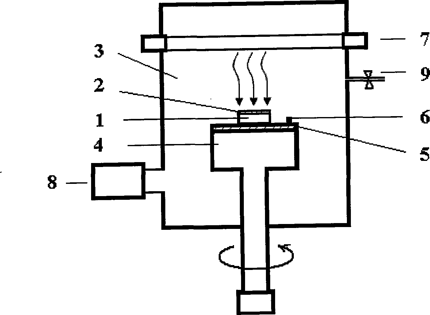
[0015] Embodiment 1: referring to accompanying drawing, at first on common glass substrate 1, use plasma-enhanced chemical vapor deposition (PECVD) to deposit a 4 inch diameter area, the amorphous silicon film 2 that thickness is 50nm; The glass substrate 1 of the crystalline silicon thin film 2 is shifted on the rotatable stage 4 in the vacuum chamber 3 (this method can obtain higher uniformity of the large-area film). A xenon excimer ultraviolet lamp 7 is installed directly above the stage in the vacuum chamber 3, providing up to 100mW / cm 2 The light intensity, the distance between the stage 1 and the excimer ultraviolet lamp 7 is 8cm, and there is a plane temperature control heating element 5 and a thermocouple temperature measuring device 6 on the stage. Turn on the vacuum pump system 8 connected to the vacuum chamber 3 to evacuate, repeatedly flush the inner wall of the vacuum chamber with an inert gas such as argon or nitrogen or neon through the inlet valve 9, maintain ...

Embodiment 2

[0016] Embodiment 2: As in Embodiment 1, wherein the light source for irradiation is a krypton excimer lamp.

Embodiment 3

[0017] Embodiment 3: as embodiment 1, wherein the irradiation light source is an argon excimer lamp.


PUM

PropertyMeasurementUnit
wavelengthaaaaaaaaaa

Abstract

The invention relates to a method for preparing lager area polysilicon by utilizing vacuum ultraviolet lamp irradiation, which is characterized in that a substrate carried with amorphous silicon membrane is positioned in the vacuum condition or the inactive atmosphere to heat, and to receive the radiation light irradiation from the vacuum ultraviolet lamp, and to cause the substrate is converted into the polysilicon through crystallization. Compared with the prior laser crystallization method, the invention has the advantages that the lamplight irradiation area is large, the speed is fast, and the crystallization conversion time is short, for example, the time for the amorphous silicon of an area with four inches diameter to convert into the polysilicon is less than an hour, and the radiation uniformity is good, not only the preparation of the large area polysilicon membrane can be easily realized, but also the uniformity and the reproducibility of the large area preparation can be ensured, the uniformity of the polysilicon membrane obtained is good, and the reproducibility is high. In addition, the irradiation equipment is simple, the cost is low, and the operation and maintenance are simple and convenient.

Description

technical field [0001] The invention relates to an improved polysilicon film manufacturing method, especially a method for preparing large-area polysilicon by irradiation with a vacuum ultraviolet lamp. Background technique [0002] In the process of preparing polysilicon thin film, the laser irradiation crystallization method only produces an instantaneous high temperature effect at a depth of 100nm thick on the surface of the film, without touching the substrate material. Therefore, cheap ordinary glass can be used as the substrate, which can greatly reduce the manufacturing cost. welcome. The preparation process is to prepare an amorphous silicon film on the substrate first, irradiate the amorphous silicon film with laser light, and use the high energy generated by the instantaneous laser pulse to melt the amorphous silicon film and then crystallize it into polysilicon. Although this method has many advantages, due to the small laser spot and small irradiation area, the ...

Claims


Application Information

Patent Timeline
Patent Type & Authority Applications(China)
IPC IPC(8): C30B28/02C30B29/06
Inventor 余建军
Owner 余建军
Why Eureka
Try Eureka