Semiconductor device and producing method thereof

A manufacturing method and semiconductor technology, applied in the direction of semiconductor devices, semiconductor/solid-state device manufacturing, semiconductor/solid-state device components, etc., can solve the problems of expanding the size of devices, reduce contact resistance, improve reliability, and reduce size Effect

Active Publication Date: 2008-07-02
SEMICON MFG INT (SHANGHAI) CORP
View PDF1 Cites 10 Cited by
  • Summary
  • Abstract
  • Description
  • Claims
  • Application Information

AI Technical Summary

Problems solved by technology

Therefore, the process of distinguishing the heavily doped source and drain regions from the lightly doped source and drain regions through the spacer is not very necessary, and the existence of the spacer also enlarges the size of the device, which is not conducive to the trend of smaller and smaller device sizes.

Method used


Image

  • Semiconductor device and producing method thereof
  • Semiconductor device and producing method thereof
  • Semiconductor device and producing method thereof

Examples


Embodiment Construction

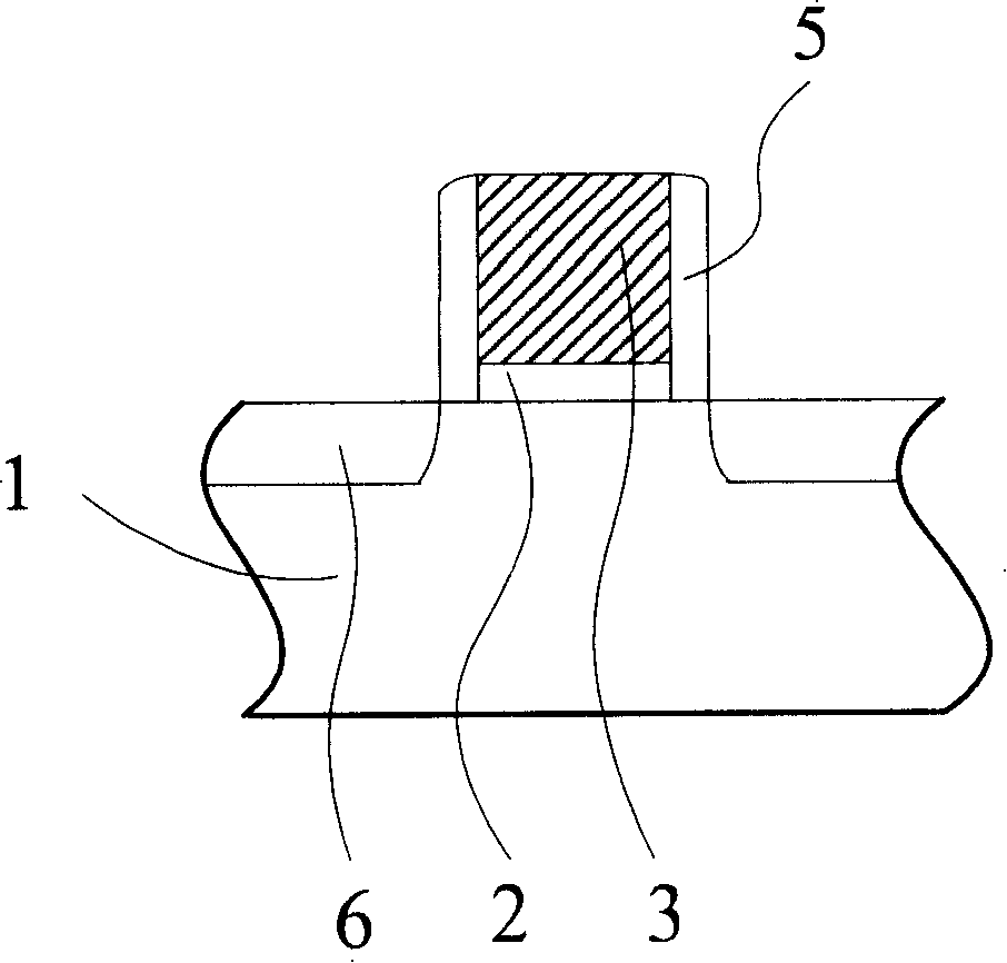
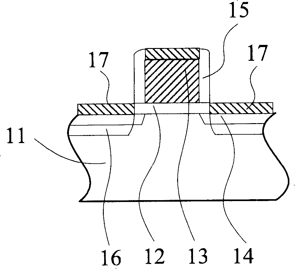
[0027] The essence of the present invention is to provide a semiconductor device without a spacer, which can be a transistor such as a memory device or a logic device, which reduces the size of the formed semiconductor device and satisfies the trend of devices becoming smaller and smaller. The region corresponding to the drain is formed with a connection interface layer extending along the surfaces of the source and drain, and the connection interface layer is a metal reactive dopant, and the dopant is oxygen, nitrogen, hydrogen, boron, arsenic or phosphorus Any one of, the metal reactive dopant is a reactive dopant of cobalt, a reactive dopant of nickel, a reactive dopant of molybdenum, a reactive dopant of titanium, a reactive dopant of copper, or niobium reactive dopants of oxygen, nitrogen, hydrogen, boron, arsenic, or phosphorus, or metal silicides containing a dopant of any of oxygen, nitrogen, hydrogen, boron, arsenic, or phosphorus, which contain continuously available ...


PUM


Abstract

The invention relates to a semiconductor apparatus comprising a semiconductor substrate, a gate dielectric layer positioned on the semiconductor substrate, a gate positioned on the gate dielectric layer as well as a source cathode and a drain positioned between the two sides of the dielectric layer in the semiconductor layer. The semiconductor apparatus also comprises a joint interface layer extending along the surface of the source cathode and drain and the joint interface layer extending along the gate surface. The joint interface layers insulate and isolate with the gate dielectric layer. The joint interface layers of the semiconductor apparatus contain doping interface providing a continuous electronic states which can complete the electron transmission under low effect of a electric field, thus reducing the contact desistence between the semiconductor and the joint metal of the contact hole. The apparatus just needs the connection between the super thin doping interface layer and the metal layer so as to further reduce the size of the semiconductor apparatus and increase the density of the semiconductor apparatus.

Description

technical field [0001] The invention relates to a semiconductor device and a manufacturing method thereof, in particular to an interconnection structure between semiconductor devices and a manufacturing method thereof. Background technique [0002] The device structure of the traditional semiconductor memory, such as the memory structure provided by the Chinese patent application number 03145409, such as figure 1 As shown, a gate dielectric layer 2 and a gate 3 are sequentially formed on a semiconductor substrate 1, the gate dielectric layer 2 is silicon dioxide or silicon oxide-silicon nitride-silicon oxide layer, etc., the gate Pole 3 is a polysilicon layer. There are spacers 5 on both sides of the gate dielectric layer 2 and the gate 3, and the material of the spacers 5 is silicon dioxide, silicon nitride or silicon oxynitride, etc., and the semiconductor substrate on both sides of the spacers 5 1 to form an active drain 6. [0003] In actual application and manufactur...

Claims


Application Information

Patent Timeline
Patent Type & Authority Applications(China)
IPC IPC(8): H01L29/78H01L29/45H01L23/522H01L21/336H01L21/28H01L21/768
Inventor 王津洲
Owner SEMICON MFG INT (SHANGHAI) CORP
Why Eureka
Try Eureka