AlSb/CIS thin film solar cell of mechanical laminated layer

A thin-film solar cell and lamination technology, which is applied in circuits, photovoltaic power generation, electrical components, etc., can solve problems such as difficult control of chemical ratio, reduced efficiency, and high work function of CdTe

Inactive Publication Date: 2008-07-09
SICHUAN UNIV
View PDF0 Cites 14 Cited by
  • Summary
  • Abstract
  • Description
  • Claims
  • Application Information

AI Technical Summary

Problems solved by technology

[0004] 1. It is difficult to prepare such ternary or multi-component compounds, and it is difficult to control the chemical ratio
[0005] 2. Especially for such ternary or multi-component compound materials as the absorbing layer of the top battery, it is necessary to replace the opaque back contact with a transparent back contact material, such as transparent conductive oxide film (TCO), but the high temperature process of preparation leads to Ga 2 o 3 The formation of TCO and the lack of components in TCO seriously affect the performance of the device, thereby greatly reducing the efficiency
First of all, CdTe is used as the absorber layer of the top battery, and its energy gap is relatively small; secondly, the work function of CdTe is very high, it is difficult to directly form an ohmic contact with the metal behind it, and it is usually necessary to add a complex composite layer to form a transparent back contact, such as ZnTe :Cu / ITO、Cu x Te / ITO

Method used


Image

  • AlSb/CIS thin film solar cell of mechanical laminated layer

Examples


Embodiment 1

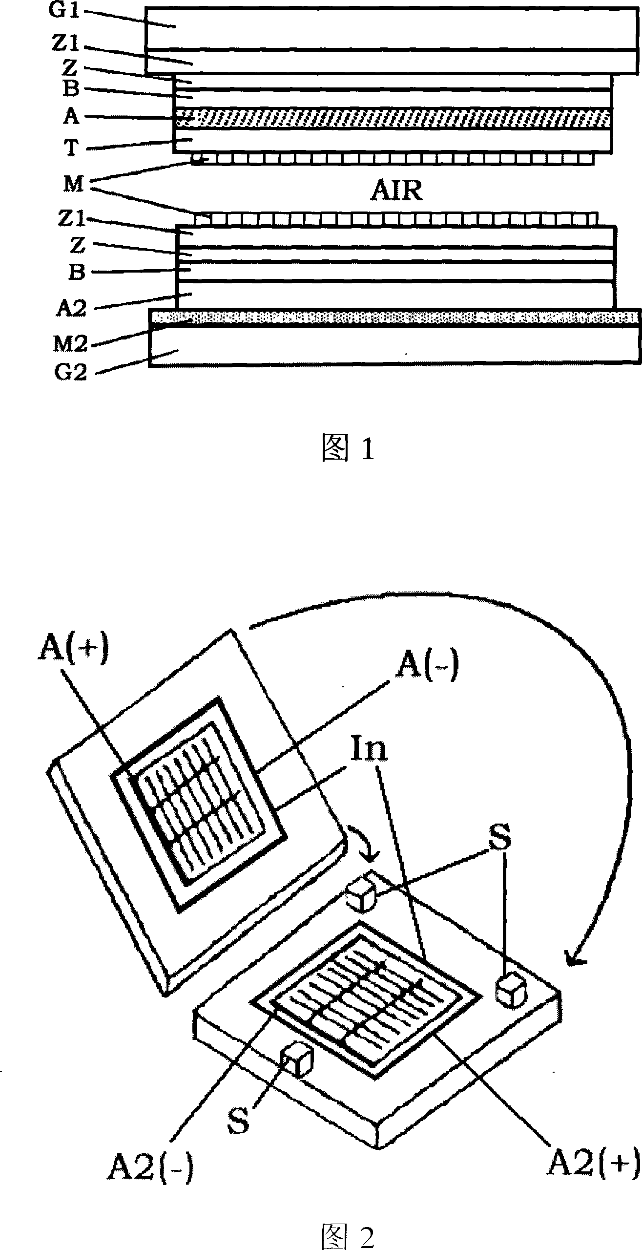
[0018] 1 Preparation of CIS (A2) bottom cell

[0019] 1.1 On Soda lime glass (G2), use a molybdenum target with a purity of 99.999%, in a background vacuum of ~10-4 Pa, the working gas is argon, the sputtering pressure is ~1Pa, and the sputtering power is 20~300W. Molybdenum (M2) with a thickness of about 0.9-1.5 μm;

[0020] 1.2 Take out the sample Soda lime glass (G2) / molybdenum (M2) after sputtering, in a vacuum of ~10 -4 Pa, adopt copper, indium, selenium three sources (purity is 99.99%) co-evaporation method to prepare CIS (A2), when sample temperature is 300 ℃, adjust the speed ratio (0.3~0.7) of copper, indium, selenium: (0.8 ~1.2):(2.2~2.6), deposit copper-rich CIS with a thickness of 0.5~1.5μm, then adjust the sample temperature to 450°C, and adjust the speed ratio to (0.1~0.5):(0.8~1.2):(1.8~2.2) , and then deposited a poor copper CIS 1.5 ~ 2.5μm;

[0021] 1.3 After the sample Soda lime glass (G2) / molybdenum (M2) / CIS (A2) is cooled, it is taken out, and the buffer...

Embodiment 2

[0034] The preparation method of ~50nm buffer layer cadmium sulfide (B) in step 1.3 and step 2.2 in embodiment 1 is changed to radio frequency sputtering method to obtain nanostructured buffer layer cadmium sulfide (B). Among them, the purity of CdS target is 99.99%, and the background vacuum is ~10 -4 Pa, the working gas is argon oxygen (oxygen 1% ~ 2%), the working pressure is 1 ~ 2Pa, the sputtering power is 30 ~ 100W, under the above conditions, the buffer layer cadmium sulfide (B ). Other processes are unchanged, the same as in Embodiment 1. Similarly, a double-junction four-terminal AlSb / CIS mechanical stack battery with a buffer layer of cadmium sulfide (B) in nanostructures can be prepared.


PUM


Abstract

The invention relates to a mechanical laminated AlSb / CIS thin film solar cell, which pertains to a structural design of a semiconductor thin film solar cell. The invention is a double-junction four-terminal thin film solar cell which is formed by mechanically superimposing an AlSb top cell on a CIS bottom cell, wherein, the AlSb top cell is the solar cell which is produced by that an n-type aluminum-doped zinc oxide conductive layer is firstly deposited on a Corning 7459 glass, then a zinc oxide high resistance layer is deposited, a cadmium sulfide buffer layer is deposited, after that, an aluminum antimonide absorption layer and a carbon nano-tube coating are deposited to be taken as a transparent conductive layer, and finally a nickel / aluminum grid line is deposited; the CIS bottom cell is the solar cell which is produced by that molybdenum is deposited on a Soda lime glass, then the absorption layer of copper indium diselenide is deposited, the buffer layer of cadmium sulfide is deposited, after that, the high resistance zinc oxide and the aluminum-doped zinc oxide are deposited, and finally the nickel / aluminum grid line with the same shape and size of the top cell is deposited. The usage of the laminated cell with the structure can selectively absorb and transform the energy of the different regions of solar spectrum, expand the scope of the response of the spectrum and effectively improve the transformation efficiency of the thin film solar cell.

Description

technical field [0001] The invention belongs to the structural design of a semiconductor thin film solar cell, in particular to a mechanically stacked thin film solar cell. Background technique [0002] Single-junction thin-film solar cells can only absorb and convert sunlight in a specific spectral range, and the photoelectric conversion efficiency is not high. If materials with different energy gap widths (Eg) are used to form double-junction or multi-junction solar cells from top to bottom according to their size, they can selectively absorb and convert energy in different regions of the solar spectrum, which can greatly improve the performance of thin-film solar cells. conversion efficiency. [0003] Coutts et al. of the US Renewable Energy Laboratory (NREL) (see Proceedings of the 12 th PhotovoltaicScience and Engineering Conference, Cheju Island, Korea, 2001: 277) calculated at AM1.5, 100mW / cm 2 , under the condition of 25°C, the efficiency of the double-junction s...

Claims


Application Information

Patent Timeline
IPC IPC(8): H01L31/042H01L31/0749H01L31/076
CPCY02E10/541Y02E10/548
Inventor 李卫冯良桓吕彬蔡亚平张静全黎兵武莉莉雷智孙震谢晗科
Owner SICHUAN UNIV
Why Eureka
Try Eureka