Organic thin-film transistor and manufacturing method thereof

A technology of organic thin film and transistor, applied in the field of organic thin film transistor and its preparation, to achieve the effect of improving injection and transmission, easy operation, and reasonable and simple preparation method

Inactive Publication Date: 2010-06-30
UNIV OF ELECTRONICS SCI & TECH OF CHINA
View PDF0 Cites 0 Cited by
  • Summary
  • Abstract
  • Description
  • Claims
  • Application Information

AI Technical Summary

Problems solved by technology

However, almost no mobility exceeds 0.1 cm 2 Instance of / Vs

Method used


Image

  • Organic thin-film transistor and manufacturing method thereof
  • Organic thin-film transistor and manufacturing method thereof
  • Organic thin-film transistor and manufacturing method thereof

Examples


Embodiment 1

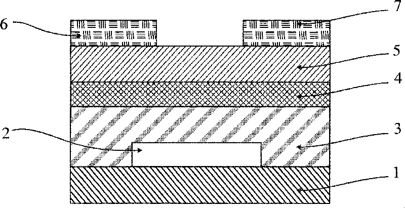
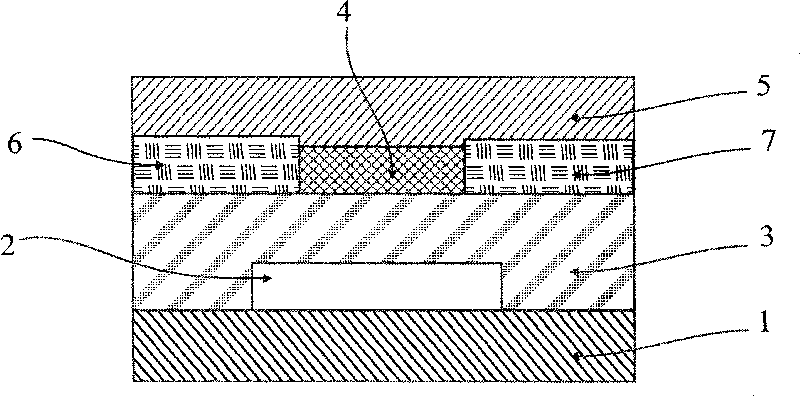
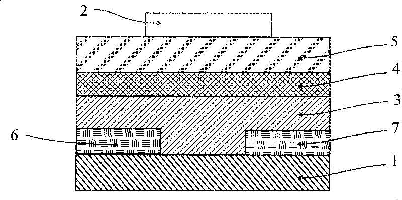
[0058] The substrate of the device is Si, the gate is Au, the insulating layer is PVP, the transition layer is PS:TPD, the organic semiconductor layer is pentacene, and the source and drain electrodes are Au.

[0059] The preparation method is as follows:

[0060] ① Thoroughly clean the Si substrate first, and blow dry with dry nitrogen after cleaning;

[0061] ② Evaporate gate electrode Au on the surface of the Si substrate by vacuum evaporation or sputtering;

[0062] ③ Etching the pattern of the gate electrode by photolithography;

[0063] ④ On the other side of the Si plate coated with the gate electrode, the organic insulating layer PVP is spin-coated by spin coating. The organic insulating layer PVP can be spin-coated into a film at one time, or it can be spin-coated on the Si substrate multiple times;

[0064] ⑤ heating and baking the spin-coated organic insulating layer PVP;

[0065] ⑥ Spin-coat the transition layer PS:TPD on the Si substrate covered with the organi...

Embodiment 2

[0069] The substrate of the device is Si, the gate is Au, the insulating layer is PVP, the transition layer is PS:NPB, the organic semiconductor layer is pentacene, and the source and drain electrodes are Au.

[0070] The fabrication process of the device is similar to that of Example 1.

[0071] Example 3

Embodiment 3

[0073] The substrate of the device is Si, the gate is Au, the insulating layer is PVP, the transition layer is CuPc, the organic semiconductor layer is pentacene, and the source and drain electrodes are Au.


PUM


Abstract

The invention provides an organic thin-film transistor, which includes: a substrate, a gate electrode, an isolation layer, an organic semiconductor layer, a leakage electrode and a source electrode. The organic thin-film transistor has structure that is one of top contact type, bottom contact type and top gate type. The organic thin-film transistor has characteristics in that: also includes a connection layer, said connection layer is composed of one or more of cavity type organic semiconductor material. Aims of the invention is to optimize manufacturing process of the organic thin-film transistor, increase the organic thin-film transistor performance, reduce greatly the organic thin-film transistor cost, and reduce technological requirement and cost for the organic thin-film transistor industrialization.

Description

technical field [0001] The invention relates to the technical field of electronic components, in particular to an organic thin film transistor and a preparation method thereof. Background technique [0002] Generally, in a flat-panel display device, elements using liquid crystal, organic EL, electrophoresis, and the like are used to form a display medium. In addition, for such display media, in order to ensure the uniformity of screen luminance and the speed of screen writing transition, etc., the technology of using active drive elements composed of thin film transistors (TFTs) as image drive elements has become mainstream. [0003] Here, TFT elements are generally manufactured by sequentially forming semiconductor thin films such as a-Si (amorphous silicon) and p-Si (polycrystalline silicon), and metal thin films such as source electrodes, drain electrodes, and gate electrodes, on a glass substrate. In recent years, the development of thin film transistors (OTFTs) using o...

Claims


Application Information

Patent Timeline
Patent Type & Authority Patents(China)
IPC IPC(8): H01L51/05H01L51/40
Inventor 于军胜李璐张磊蒋亚东
Owner UNIV OF ELECTRONICS SCI & TECH OF CHINA
Why Eureka
Try Eureka