

Improved phase change memory unit component structure
A technology of phase change memory and device structure, which is applied in the field of micro-nano electronics, can solve the problem of insufficient heating efficiency, and achieve the effects of low power consumption, uniform thermal field, low power consumption and high-speed storage
- Summary
- Abstract
- Description
- Claims
- Application Information
AI Technical Summary
Problems solved by technology
Method used
Image

Examples
Embodiment 1
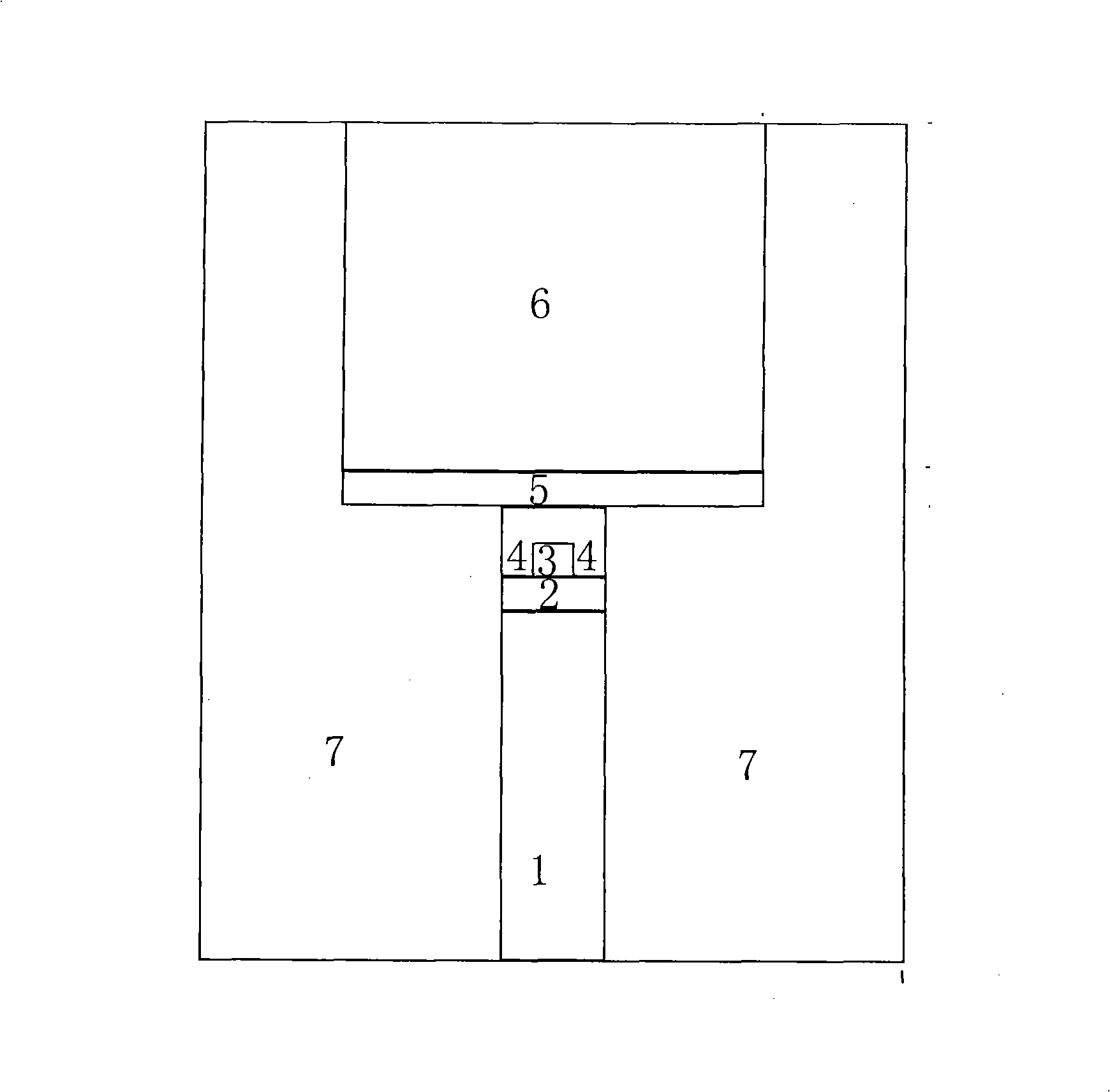
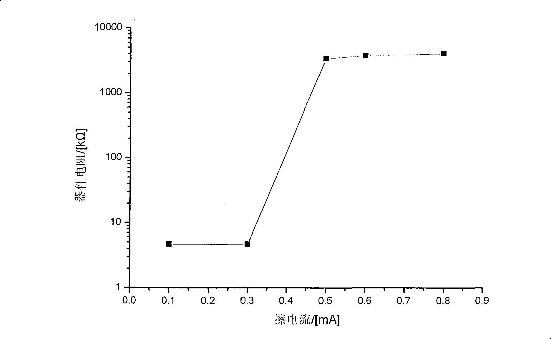
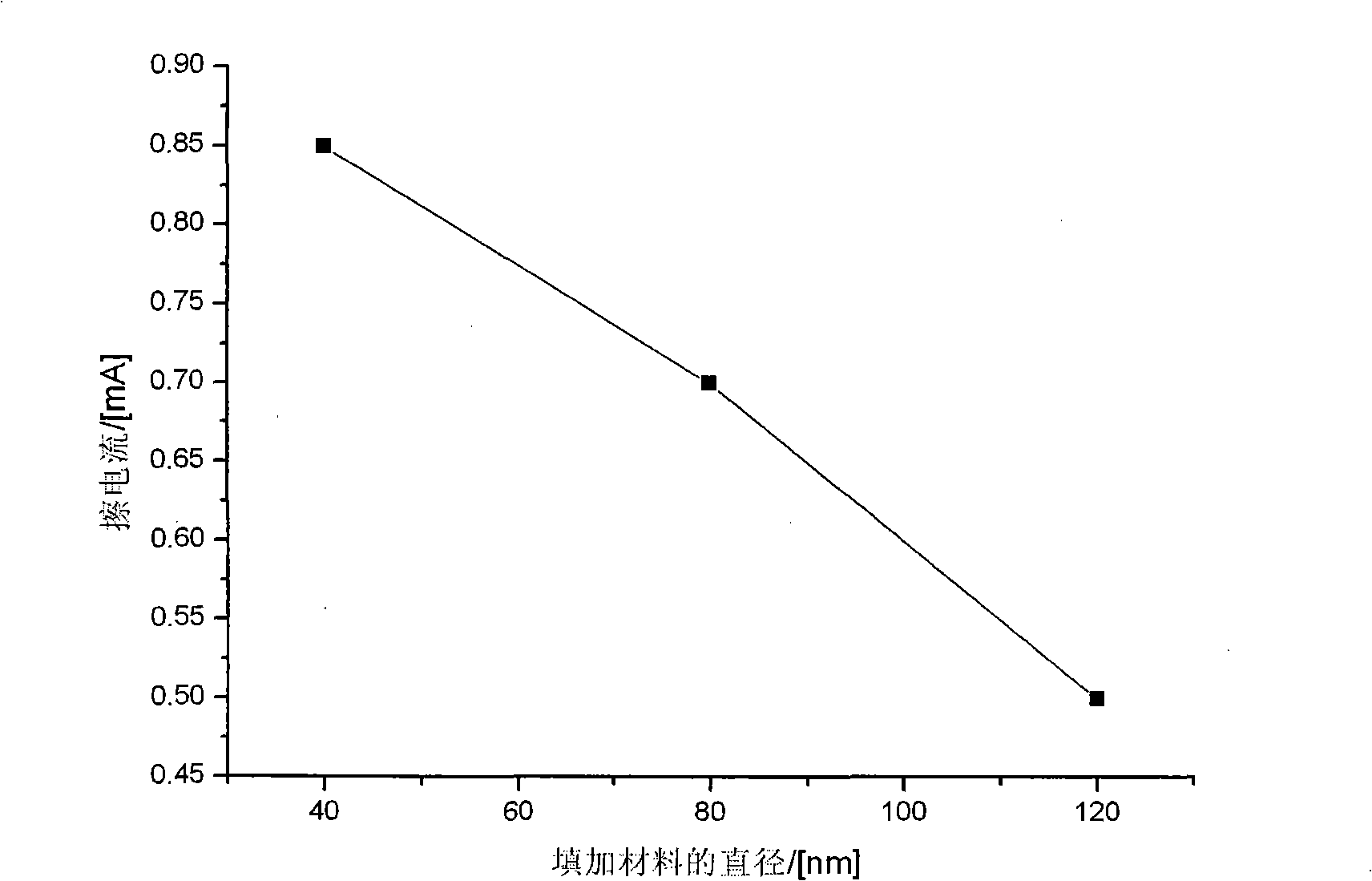
[0023] The cross-sectional structure of the device is as figure 1 . The electrode material 1 is W, the heating electrode 2 material is TiN, the phase change material 4 is GST, and the filling material 3 is SiO 2 , the material of the upper contact electrode 5 is TiN, the material of the upper electrode 6 is W, and the surrounding insulating material 7 is SiO 2 . The added material has a diameter of 120nm and a thickness of 60nm. The preparation process is as follows:
[0024] 1. Prepare lower electrode through holes on the substrate (including MOS impurity diffusion regions, source and drain regions, electrode leads, through holes, or PN diodes, bipolar transistors, etc.), the size of which is adjusted according to process conditions, and the size of the through holes can be adjusted Larger or smaller than the size of the phase change material hole, then deposit the lower electrode in the hole, such as W, TiN, silicide and other conductive media to form a metal plug.
[002...
Embodiment 2
[0030] The cross-sectional structure of the device is as Image 6 . exist Image 6 In the example, 1 is the lower electrode W, 2 is BEC, and the heating electrode material 3 is SiO 2 Insulation material, 4 is phase change material such as GST, 5 is TEC upper contact electrode material, 6 is upper electrode W, 7 is SiO 2 . Compared with Example 1, the structure process is complicated, but the thermal efficiency is higher.
[0031] The preparation process is as follows:
[0032] 1. Prepare lower electrode through holes on the substrate (including MOS impurity diffusion regions, source and drain regions, electrode leads, through holes, or PN diodes, bipolar transistors, etc.), the size of which is adjusted according to process conditions, and the size of the through holes can be adjusted Larger or smaller than the size of the phase change material hole, and then deposit the lower electrode in the hole, such as W, TiN or silicide and other conductive media to form a metal plu...
PUM
| Property | Measurement | Unit |
|---|---|---|
| Diameter | aaaaa | aaaaa |
| Thickness | aaaaa | aaaaa |
| Thickness | aaaaa | aaaaa |
Abstract
Description
Claims
Application Information