Process and device for removing phosphorus and metal impurities in polycrystalline silicon

A technology of metal impurities and polysilicon, applied in chemical instruments and methods, non-metallic elements, silicon compounds, etc., can solve the problems of low primary conversion rate, high energy consumption, long process time, etc., to save energy, improve purity, and install simple effect

Inactive Publication Date: 2008-10-22
QINGDAO NEW ENERGY SOLUTIONS
View PDF1 Cites 39 Cited by
  • Summary
  • Abstract
  • Description
  • Claims
  • Application Information

AI Technical Summary

Problems solved by technology

The disadvantage of the Siemens method is that it adopts backward thermal chemical vapor deposition in the core link of the process. There are too many links in the process and the conversion rate is low at one time, which leads to a long process time and increases the cost of materials and energy consumption.
The simple directional solidification method cannot remove the impurity phosphorus with a large segregation coefficient. Among the many impurities in polysilicon, phosphorus is a harmful impurity, which directly affects the resistivity and minority carrier lifetime of silicon materials, and then affects the performance of solar cells. Photoelectric conversion efficiency
The phosphorus content of polycrystalline silicon that can be used to prepare solar cells is required to be reduced to less than 0.0001%. It is known that the invention patent of Japanese Patent No. 11-20195 uses electron beams to achieve the purpose of removing phosphorus in polycrystalline silicon, but the disadvantage of this invention is that it uses two electron guns Large energy consumption, no directional solidification system can not remove other metal impurities

Method used


Image

  • Process and device for removing phosphorus and metal impurities in polycrystalline silicon

Examples


Embodiment Construction

[0019] Specific embodiments of the solution will be described in detail below in conjunction with the technical solution and accompanying drawings.

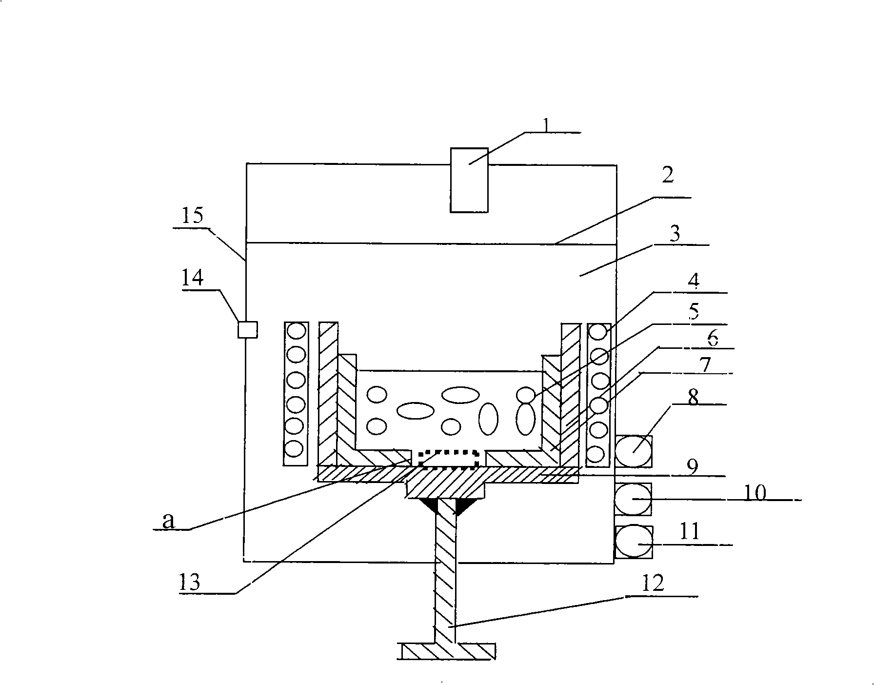
[0020] Spread silicon powder 13 with a high purity of 99.9999% on the water-cooled copper base 9 and fill the hollow space a of the quartz crucible 7 . Put the polysilicon material 5 with a purity of 99.8% in which impurity phosphorus content is 0.005%, iron content is 0.1254%, and aluminum content is 0.0342% into a quartz crucible 7, and the vacuum device cover 2 is closed. In the vacuuming process, the vacuum chamber 3 is first pumped to a low vacuum 10 with a mechanical pump 8 and a Rhodes pump 10. -0 pa, then use diffusion pump 11 to pump the vacuum to high vacuum 10 -3 below pa. Set the power to 10kW to energize the induction coil 4, and the temperature reaches 1500°C to melt all the silicon material. Preheat the electron gun 1 with 100mA, preheat the beam for 5 minutes, turn off the beam of the electron gun 1, then reduc...


PUM

PropertyMeasurementUnit
diameteraaaaaaaaaa

Abstract

The invention relates to a method and a device for removing impurity phosphorus and metal impurities in polycrystalline silicon, which pertains to the technical field of purifying the polycrystalline silicon by a physical metallurgy technology, particularly relates to the method for removing the impurity phosphorus and the metal impurities in the polycrystalline silicon by an electron-beam fusion technology. Cooperative ways of electron-beam fusion and induction heating are used for completing the fusion and solidification process of the polycrystalline silicon. Silicon powder with high purity is used for spreading in a hollow-out space at a water cooled copper base which is filled with quartz crucibles; polycrystalline silicon material is put into the quartz crucibles and the cover of a vacuum device is closed; in the process of vacuumization, a mechanical pump and a lodz pump are firstly used for vacuumizing a vacuum room to low vacuum and then a diffusion pump is used for vacuumizing to high vacuum; the device used is provided with a vacuum device cover and a vacuum drum which are formed into the outer shell of the device; the inner cavity of the vacuum drum is the vacuum room, in which a fusion system is arranged. The method and the device of the invention effectively improve the purity of the polycrystalline silicon, which have the advantages of high efficiency, simple device and saving energy.

Description

technical field [0001] The invention belongs to the technical field of purifying polysilicon by using physical metallurgy technology, and in particular relates to a method for removing impurity phosphorus and metal impurities in polysilicon by electron beam smelting technology. Background technique [0002] High-purity polysilicon is the main raw material for solar cells. The preparation of high-purity polysilicon abroad mainly uses the Siemens method, specifically the silane decomposition method and the gas-phase hydrogen reduction method of chlorosilane, in which SiHCl 3 The Siemens method is currently the mainstream technology for polysilicon preparation. SiHCl 3 The useful deposition ratio of the method is 1×10 3 , is SiH 4 100 times. The deposition rate of the Siemens method can reach 8-10 μm / min. The conversion efficiency of one pass is 5% to 20%, and the deposition temperature is 1100°C, second only to SiCl 4 (1200°C), the power consumption is about 120kWh / kg, ...

Claims


Application Information

Patent Timeline
Patent Type & Authority Applications(China)
IPC IPC(8): C01B33/037
CPCY02P20/10
Inventor 谭毅李国斌姜大川许富民王强
Owner QINGDAO NEW ENERGY SOLUTIONS
Why Eureka
Try Eureka