Passivation layer of IC chip

A technology of integrated circuits and passivation layers, applied in circuits, electrical components, electrical solid devices, etc., can solve problems such as peeling off, failure of integrated circuit devices, and poor adhesion, and achieve the effect of improving yield

Active Publication Date: 2008-11-12
SEMICON MFG INT (SHANGHAI) CORP +1
View PDF0 Cites 6 Cited by
  • Summary
  • Abstract
  • Description
  • Claims
  • Application Information

AI Technical Summary

Problems solved by technology

Due to the difference between the Young's modulus and the coefficient of thermal expansion of the first SiO2 layer 3 and the SiN layer 1, the first SiO2 under the above process 2 Both layer 3 and SiN layer 1 exert shrinkage stress on the metal layer, resulting in poor adhesion between the passivation layer and the metal layer, and between the metal layer and the dielectric insulating layer, forming peeling (Peeling) peeling off, and finally causing integrated circuit devices failure of

Method used


Image

  • Passivation layer of IC chip
  • Passivation layer of IC chip

Examples


Embodiment Construction

[0021] The present invention will be described in detail below in conjunction with the accompanying drawings and specific embodiments.

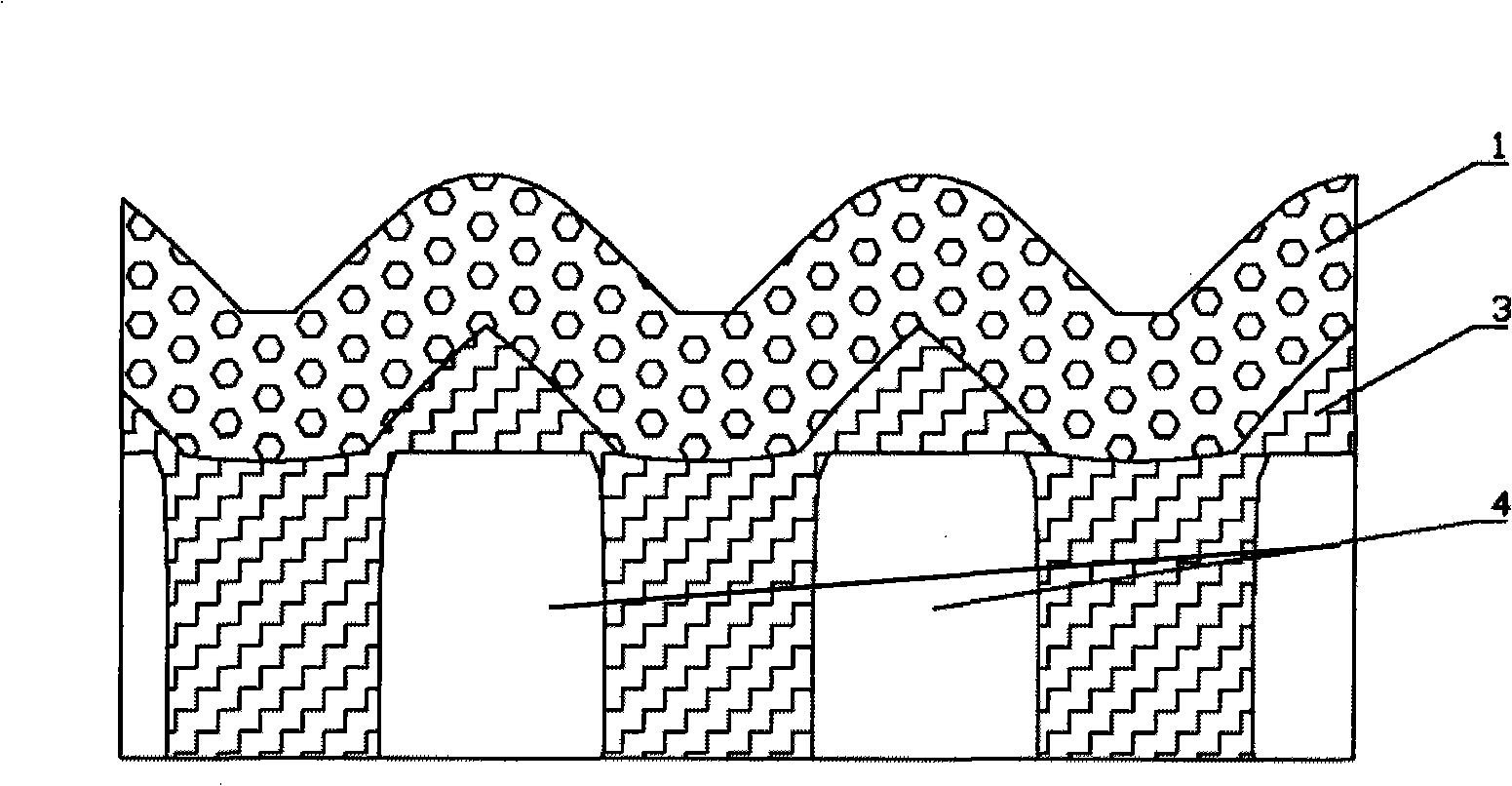
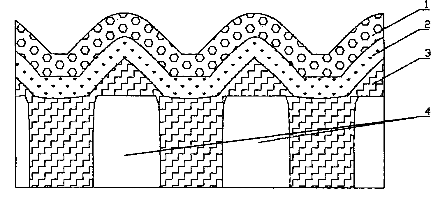
[0022] see figure 2 , the invention discloses a passivation layer of an integrated circuit chip, comprising at least a first SiO 2 Layer 3, second SiO 2 Layer 2 and SiN layer 1. Second SiO 2 Layer 2 is located on the first SiO 2 Between layer 3 and SiN layer 1.

[0023] First SiO 2 Layer 3 is formed by a high-density plasma chemical vapor deposition (HDPCVD) process or a plasma-enhanced chemical vapor deposition (PECVD) process, and the first SiO 2 Both layer 3 and SiN layer 1 exert shrinkage stress on the metal layer. In the present invention, the thickness of both and SiO in the prior art 2 layer is the same thickness as the SiN layer.

[0024] Second SiO 2 Layer 2 is produced by a sub-atmospheric chemical vapor deposition (SACVD) process, usually with ozone (O 3 ) and tetraethyl orthosilicate (TEOS) chemical reaction, depositio...


PUM


Abstract

The invention provides a passivant layer of an integrated circuit chip, which comprises at least a first silicon dioxide layer and a silicon nitride layer, wherein the first silicon dioxide is positioned under the silicon nitride layer; the invention is characterized in that the passivant layer also comprises a second silicon dioxide layer which is positioned between the first silicon dioxide layer and the silicon nitride layer. The passivant layer of the invention can effectively avoid a peeling off and dropping off between the passivant layer and a metal layer, between the metal layer and a medium insulating layer, thus improving yield of integrated circuit chips.

Description

technical field [0001] The invention belongs to the field of chip manufacturing, in particular to a passivation layer (Passivation) of an integrated circuit chip. Background technique [0002] The surface passivation of integrated circuits can reduce various charges in the oxide layer, enhance the device's ability to resist ion contamination, and protect circuits and internal interconnections from mechanical and chemical damage. Due to the difference in Young's modulus and thermal expansion coefficient of each layer of material, in the process of integrated circuit preparation, such as deposition, polishing, sputtering, photolithography, etc., the stress inside the film will change due to the corresponding temperature change, thus forming Voids, cracks or falling off, causing deformation of the integrated circuit structure and short circuit or open circuit of interconnection wires, resulting in device failure. [0003] The type and structure of the passivation layer have a ...

Claims


Application Information

Patent Timeline
Patent Type & Authority Applications(China)
IPC IPC(8): H01L27/02H01L23/00H01L21/71H01L21/314
Inventor 曾建平董梅马琳
Owner SEMICON MFG INT (SHANGHAI) CORP
Why Eureka
Try Eureka