Production method of surface conducting polymer graphic pattern

A kind of conductive polymer and polymer technology, applied in the direction of photoplate making process of pattern surface, optical mechanical equipment, nanostructure manufacturing, etc., can solve the problems of high cost and long time, and achieve mature technology, simple process and high production rate high effect

Inactive Publication Date: 2008-12-10
JILIN UNIV
View PDF0 Cites 12 Cited by
  • Summary
  • Abstract
  • Description
  • Claims
  • Application Information

AI Technical Summary

Problems solved by technology

High-resolution patterns require high-resolution templates, which requires a long and costly template preparation process

Method used


Image

  • Production method of surface conducting polymer graphic pattern
  • Production method of surface conducting polymer graphic pattern
  • Production method of surface conducting polymer graphic pattern

Examples


Embodiment 1

[0049]The aniline monomer can be oxidatively polymerized into polyaniline under the condition of ferric chloride as an oxidizing agent, and can form a uniform film on the substrate. We added N-(3-trimethoxypropyl)pyrrole monomer to the polymerization system to copolymerize with aniline, which strengthened the adhesion ability of the polyaniline film to the substrate.

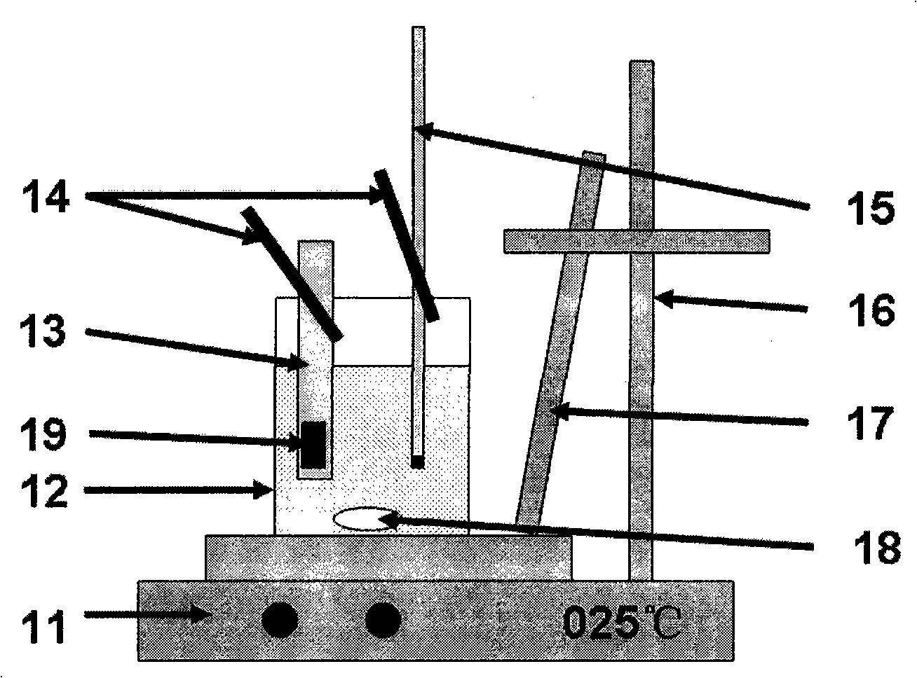
[0050] Preparation conditions of polyaniline film:

[0051] Aniline 1mL, N-(3-trimethoxypropyl)pyrrole monomer 40μL, iron trichloride 0.72g, temperature 25°C, time 10min.

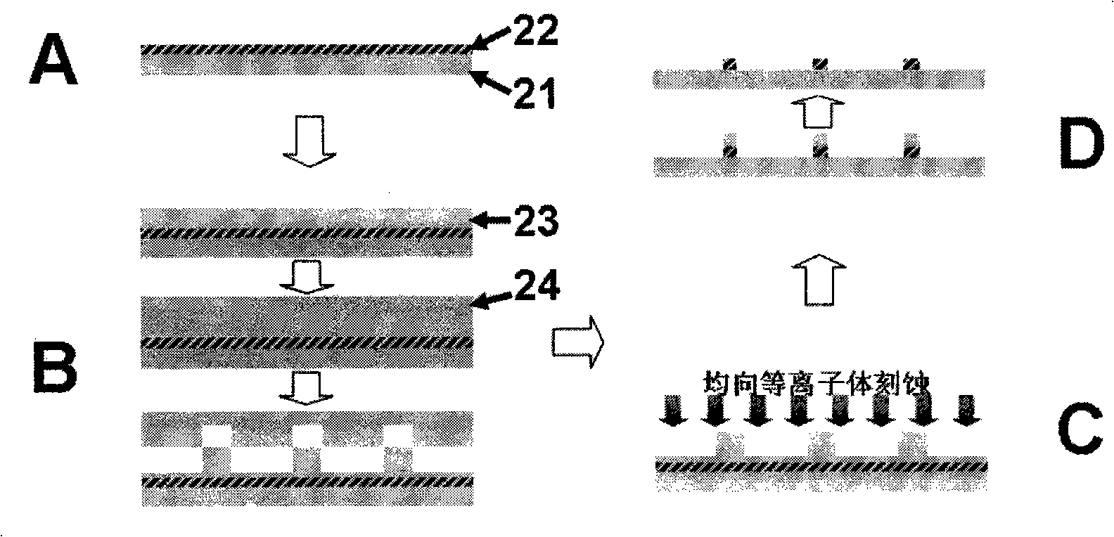
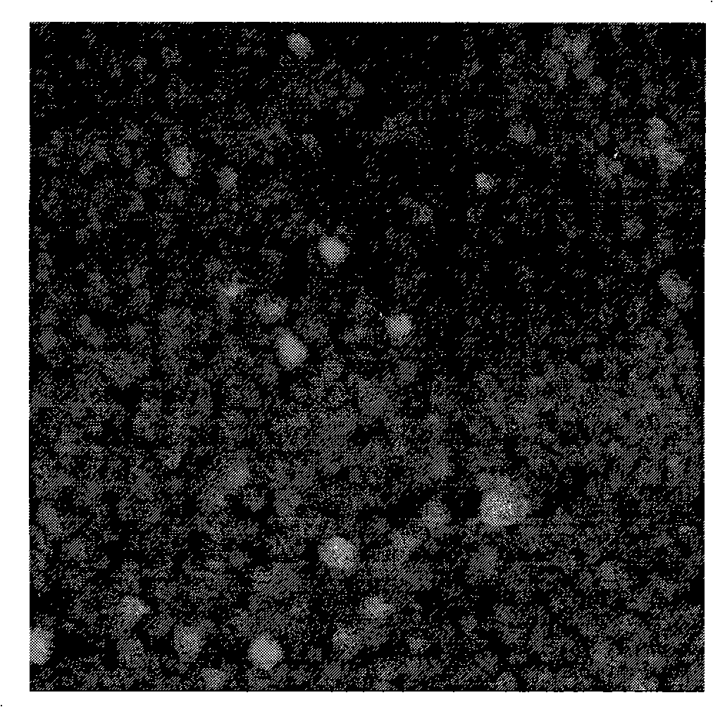
[0052] The morphology of polyaniline thin films was characterized by tapping mode of atomic force microscope, as image 3 shown. It can be seen from the figure that polyaniline can form a uniform film on the silicon dioxide substrate, the film thickness is 20nm, and the surface roughness is about 7.157nm. Then spin-coat PMMA film (400nm) on this layer of film, and anneal at 120°C for 5min. Imprinting uses a strip patterned silicon templat...

Embodiment 2

[0054] The polyaniline sample that is spin-coated with the PMMA thin film with the silicon template (such as the positive type (raised square pattern) pattern) that handles in embodiment 1 Figure 8 shown) for imprinting. The specific fluorination process of the silicon template is as follows: the surface of the template is treated with an oxygen plasma system, the oxygen flow rate is 120mL / min, the power is 300W, and the treatment time is 3 minutes; then the surface of the template is ultrasonically cleaned with high-purity water for 3 times, each time is 5 minutes , so that the surface was thoroughly cleaned; then the template was dried at 120°C for 1 h, and finally a layer of fluorosilylating reagent (perfluorodecyl-1, 1,2,2-Tetrahydro-trichlorosilane). The embossing conditions were controlled at a temperature of 170° C., a pressure of 50 bar, and a time of 500 s. like Figure 9 As shown, the sample is separated from the template after imprinting, and a "well" pattern th...

Embodiment 3

[0056] When the pyrrole monomer is used as an oxidizing agent in ferric chloride, a similar polymerization reaction can also occur to form a film.

[0057] Preparation conditions of polypyrrole membrane:

[0058] Pyrrole 400 μL, N-(3-trimethoxypropyl)pyrrole monomer 40 μL, ferric chloride 0.72 g, temperature 25° C., time 10 min.

[0059] Then spin-coat PMMA film (400nm) on this layer of film (its thickness is 20nm), and anneal at 120°C for 5min. The embossing conditions were controlled at a temperature of 170° C., a pressure of 50 bar, and a time of 500 s. A silicon template with a stripe pattern was used for imprinting, and its fluorination process was as in Example 1. After imprinting, the sample is separated from the template to obtain a band pattern that is completely complementary to the template structure. It is then etched with oxygen plasma. The etching conditions are controlled as an oxygen flow rate of 120ml / min, a power of 30W, and an etching time of 10min. The...


PUM

PropertyMeasurementUnit
thicknessaaaaaaaaaa
diameteraaaaaaaaaa
thicknessaaaaaaaaaa

Abstract

The invention belongs to the technology of the functional material surface patterning, in particular to a preparation method for surface conducting polymer patterns. The method is that a conducting polymer thin film formed on the base surface by the method of spin coating or oxidation polymerization; then patterns are imprinted on the polymer barrier layer of the conducting polymer thin film through the nano-imprint; isotropic etching is carried out with the patterns as the masks, and thus the surface conducting polymer patterns with controllable structure and size are prepared on the base surface. The problem that the high density and high productivity are not simultaneous is solved by the method. On the basis, the resolution of the surface conducting polymer patterns is several times higher than that of the masks. The invention has the characteristics of low cost, high efficiency and mature technology, is coincidence with the industrialization standards, and can be used for making optical, electronic, magnetic and biological devices as well as producing sensors and dischargeable batteries; the application ability of the functional materials such as the conducting polymer, etc., is greatly improved.

Description

technical field [0001] The invention belongs to the surface pattern construction technology of functional materials, and specifically relates to a method for preparing a surface conductive polymer pattern, which is to form a thin film of conductive polymer on the surface of a substrate by means of spin coating or oxidative polymerization, and then transfer the spin coating to the surface by nanoimprinting. The polymer barrier layer coated on the conductive polymer film is embossed with a pattern, and the imprinted pattern is used as a mask to carry out homogeneous etching, so as to prepare a surface conductive polymer pattern with controllable structure size on the surface of the substrate. Background technique [0002] Conductive polymer is not only a unique material with electrical, optical and magnetic properties, but also has excellent mechanical processing properties, such as light weight, easy processing, and good bendability, so it has attracted widespread attention. ...

Claims


Application Information

Patent Timeline
Patent Type & Authority Applications(China)
IPC IPC(8): G03F7/00B82B3/00C08G73/02C08G73/06C08G61/12
Inventor 吕男黄春玉董彬高立国杨秉杰齐殿鹏田露吴琼迟力峰
Owner JILIN UNIV
Why Eureka
Try Eureka