ZnO based LED of multiple quantum wells
A technology of light-emitting diodes and multi-quantum well layers, which is applied to electrical components, circuits, semiconductor devices, etc., can solve problems that have not been developed before, achieve good crystal quality, reduce lattice mismatch, and improve hole injection efficiency.
- Summary
- Abstract
- Description
- Claims
- Application Information
AI Technical Summary
Problems solved by technology
Method used
Image
Examples
Embodiment 1
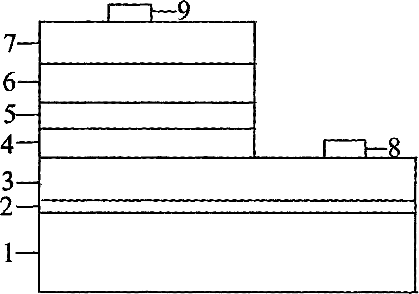
[0020] 1) Use a 2-inch monocrystalline silicon (111) polished wafer as the substrate, first use alcohol to ultrasonically clean, and then use HF to clean the natural oxide layer on the surface. Then put the substrate into the growth chamber of the pulsed laser deposition system, and the growth chamber is evacuated to 6×10 -4 pa. Then heat the substrate to 300°C, adjust the oxygen mass flow meter to control the oxygen pressure at 0.1Pa, set the laser parameters to 280mJ, 5Hz, and deposit a layer of 50nm ZnO buffer layer 2 under these conditions.
[0021] 2) Raise the temperature to 600°C and keep the oxygen pressure constant, deposit 1000nm of Al-doped n-type ZnO film layer 3 and 400nm of Al-doped n-type ZnO in sequence 0.8 Mg 0.2 O confinement layer 4, alternately deposited Zn 0.9 Mg 0.1 O layer and Zn 0.95 Cd 0.05 O layer, forming 7 periods of multi-quantum well layer 5, in this example, Zn 0.9 Mg 0.1 O layer and Zn 0.95 Cd 0.05 O layer lattice mismatch degree is 0. ...
Embodiment 2
[0026]1) With a 2-inch ZnO single crystal as the substrate, first use alcohol to ultrasonically clean it, and then use HF to clean the natural oxide layer on the surface. Then put the substrate into the growth chamber of the pulsed laser deposition system, and the growth chamber is evacuated to 2×10 -4 pa. Then heat the substrate to 400°C, adjust the oxygen mass flow meter to control the oxygen pressure at 0.5Pa, set the laser parameters to 280mJ, 5Hz, and deposit a layer of 50nm ZnO buffer layer 2 under these conditions.
[0027] 2) Raise the temperature to 600°C and keep the oxygen pressure constant, deposit 1000nm of Al-doped n-type ZnO film layer 3 and 400nm of Al-doped n-type ZnO in sequence 0.6 Mg 0.4 O confinement layer 4, alternately deposited Zn 0.7 Mg 0.3 O layer and Zn 0.9 Cd 0.1 O layer, forming 10 periods of multi-quantum well layer 5, in this example, Zn 0.7 Mg 0.3 O layer and Zn 0.9 Cd 0.1 O layer lattice mismatch degree is 0. Then deposit 200nm of Na-...
Embodiment 3
[0030] 1) With a 2-inch ZnO single crystal as the substrate, first use alcohol to ultrasonically clean it, and then use HF to clean the natural oxide layer on the surface. Then put the substrate into the growth chamber of the pulsed laser deposition system, and the growth chamber is evacuated to 5×10 -5 pa. Then heat the substrate to 400°C, adjust the oxygen mass flow meter to control the oxygen pressure at 20Pa, set the laser parameters to 280mJ, 5Hz, and deposit a layer of 50nm ZnO buffer layer 2 under these conditions.
[0031] 2) Raise the temperature to 600°C and keep the oxygen pressure constant, deposit 800nm Al-doped n-type ZnO film layer 3 and 400nm Al-doped n-type ZnO film in sequence 0.7 Mg 0.3 O confinement layer 4, alternately deposited Zn 0.8 Mg 0.2 The O layer and the ZnO layer form a multi-quantum well layer 5 with 16 periods. In this example, Zn 0.8 Mg 0.2 The degree of lattice mismatch between the O layer and the ZnO layer is less than 5%. Then deposi...
PUM
 Abstract
Description
Claims
Application Information


