CdS nano rod growth method by catalyst-assisted and vacuum heat evaporation

A vacuum evaporation and catalyst technology, applied in the direction of cadmium sulfide, etc., can solve the problems of not preparing cadmium sulfide nanorods, difficult nanostructures, and difficult control, etc., to avoid impurities and other by-products, large deposition area, and simple method Effect

Inactive Publication Date: 2009-04-01
XINJIANG UNIVERSITY
View PDF0 Cites 14 Cited by
  • Summary
  • Abstract
  • Description
  • Claims
  • Application Information

AI Technical Summary

Problems solved by technology

[0004] It can be seen that the typical materials for the preparation of nanorods by thermal evaporation are metal oxides, and there is no report on the preparation of cadmium sulfide nanorods. The preparation of cadmium sulfide nanorods by chemical vapor deposition requires the introduction of reaction gas and carrier gas, which is difficult to control and very difficult. It is difficult to obtain large-area uniform nanostructures on various substrates

Method used


Image

  • CdS nano rod growth method by catalyst-assisted and vacuum heat evaporation
  • CdS nano rod growth method by catalyst-assisted and vacuum heat evaporation
  • CdS nano rod growth method by catalyst-assisted and vacuum heat evaporation

Examples


Embodiment 1

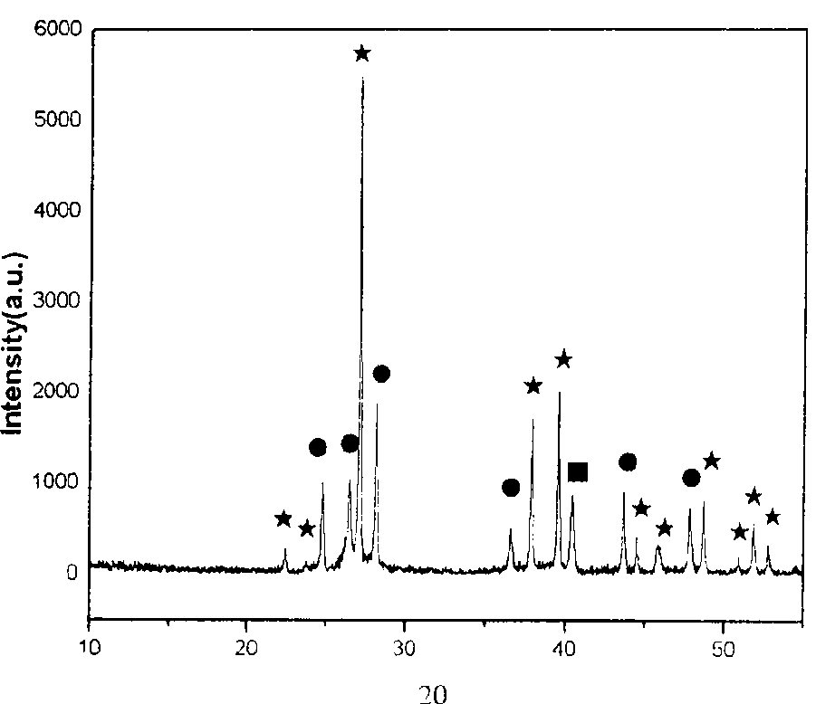
[0017] Use high-purity CdS powder (99.5%) as raw material and high-purity metal bismuth powder as catalyst. After the two are uniformly mixed at 1mol:0.125mol, the powder is directly placed on the molybdenum sheet heater, and another molybdenum sheet is used as the lining. The bottom is placed about 5mm above the evaporation source. When the vacuum reaches 8×10 -3 After Pa, the evaporation chamber was sealed, and the current was gradually increased to 130 A at a current increase rate of 2.5 A / min and then kept for 10 minutes. There are yellow deposits on the bottom surface. The surface morphology of the substrate deposits observed by SEM is pin-shaped nanorods, the bulk of which is 500-800nm ​​particles, and the diameter of the nanorods connected to the particles is gradually reduced from 300-500nm, and the rod length is 3-5μm, such as figure 2 . The XRD analysis results show that the main phase of the product is hexagonal CdS, and the catalyst is hexagonal Bi, such as fi...

Embodiment 2

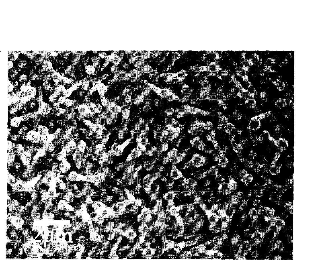
[0019] Using high-purity CdS powder (99.5%) as raw material, high-purity metal bismuth powder as a catalyst, after the two are uniformly mixed in a ratio of 1mol:0.04mol, the obtained powder is directly placed on the molybdenum sheet heater, and the ITO glass is The substrate was placed approximately 2 cm above the evaporation source. When the vacuum reaches 8×10 -3 After Pa, the evaporation chamber was sealed, and the current was gradually increased to 130A at a current increase rate of 2.5A / min and then kept for 15 minutes. There are yellow deposits on the substrate surface. The surface morphology of substrate deposits observed by SEM is nanorods with a length of 1-2 μm and a diameter of 50-60 nm, such as image 3 .

Embodiment 3

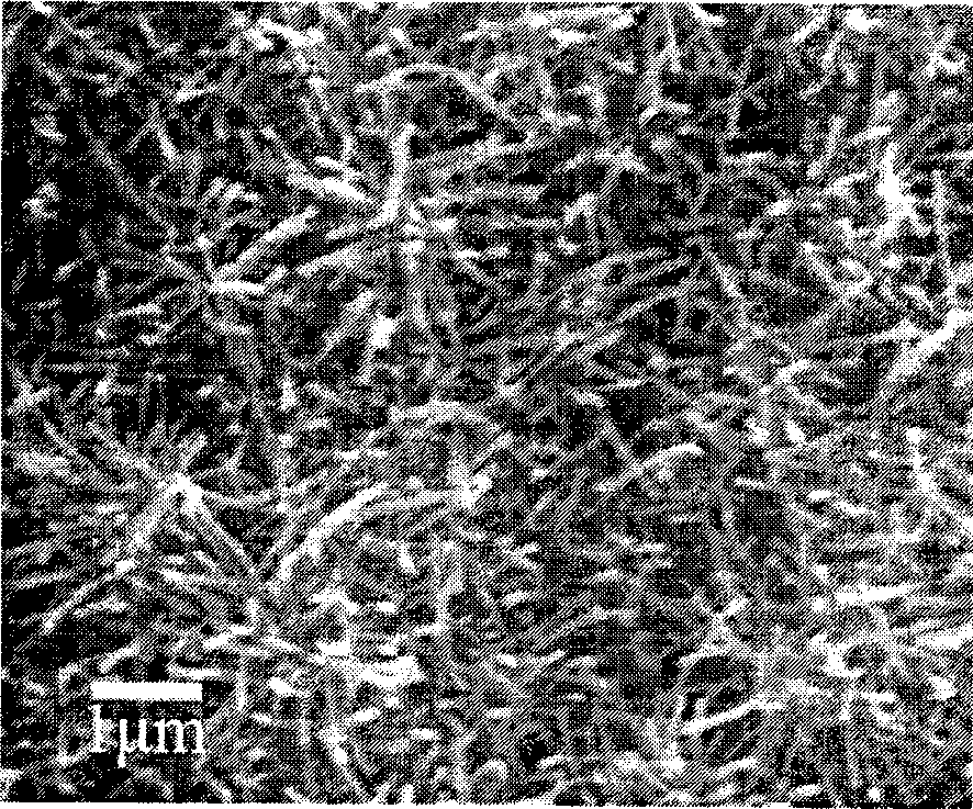
[0021] Use high-purity CdS powder (99.5%) as raw material and high-purity metal bismuth powder as catalyst. After the two are uniformly mixed at a ratio of 1mol:0.312mol, the powder is directly placed on the molybdenum heater, and the silicon wafer is used as the substrate. Place about 1cm above the evaporation source. When the vacuum reaches 8×10 -3 After Pa, the evaporation chamber was sealed, and the current was gradually increased to 130A at a current increase rate of 2.5A / min for 15 minutes. There are yellow deposits on the substrate surface. The surface morphology of the sediment observed by SEM is a uniform distribution of nanorods with a length of 5-10 μm and a diameter of 100-200 nm, such as Figure 4 .


PUM

PropertyMeasurementUnit
lengthaaaaaaaaaa
lengthaaaaaaaaaa
lengthaaaaaaaaaa

Abstract

The invention discloses a method for growing a CdS nano rod of II-VI semiconductor compound by vacuum and thermal evaporation and assistance by catalysts, and is realized by the following processes: CdS powder and metal Bi powder are mixed evenly as per the proportion of mol ratio of 1 : 0.01 - 1 : 0.35 for preparing the raw material, placed in a resistance heating boat made of molybdenum sheets, and various substrates are placed 3 mm - 3 cm over the boat. After the cavity of the vacuum evaporation furnace of the evaporation sedimentation system which is placed internally reaches the vacuum environment of 2*10<-2>-2*10<-3>Pa, the evaporation furnace is sealed, 100-180A of current is led to the resistance heating boat for 5-15 minutes and then evaporation and sedimentation are proceeded. The nano rod of cadmium sulphide prepared by the invention is crystal-stated hexagonal-phase-structured CdS. The nano bod of cadmium sulphide of the invention is characterized by being applicable to various substrates, large segment area and even feature; and the method of the invention is simple, can be promoted easily and is applicable to a large scale of industrial production.

Description

technical field [0001] The invention belongs to the field of nanostructure growth, and in particular relates to a catalyst-assisted vacuum thermal evaporation growth method whose microscopic morphology is nanorod CdS. Background technique [0002] CdS belongs to group II-VI semiconductor materials, and like other semiconductor materials in this group, it is a direct energy gap semiconductor. The band gap at room temperature is 2.42 electron volts, which belongs to the category of visible light. In the field of optoelectronics, it is a very important semiconductor material that can be used to build nonlinear optical devices and light-emitting diodes. At the same time, it is also a good photoactive waveguide and electroluminescent material, which can be widely used in communication, information storage, and highly integrated chemical or biological sensors. In recent years, the development of nanomaterials shows that nanoscale materials are likely to have more excellent proper...

Claims


Application Information

Patent Timeline
Patent Type & Authority Applications(China)
IPC IPC(8): C01G11/02
Inventor 简基康邹华吴荣孙言飞郑毓峰
Owner XINJIANG UNIVERSITY
Why Eureka
Try Eureka